DS90CR216MTD/NOPB National Semiconductor, DS90CR216MTD/NOPB Datasheet
DS90CR216MTD/NOPB
Specifications of DS90CR216MTD/NOPB
*DS90CR216MTD/NOPB
DS90CR216MTD
Available stocks


Related parts for DS90CR216MTD/NOPB

DS90CR216MTD/NOPB Summary of contents
Page 1
... Block Diagrams DS90CR215 Order Number DS90CR215MTD See NS Package Number MTD48 TRI-STATE® registered trademark of National Semiconductor Corporation. © 2009 National Semiconductor Corporation DS90CR215/DS90CR216 The 21 CMOS/TTL inputs can support a variety of signal combinations. For example, five 4-bit nibbles plus 1 control, or two 9-bit (byte + parity) and 3 control. ...
Page 2
Connection Diagrams DS90CR215 Typical Application www.national.com 1290921 2 1290922 DS90CR216 1290923 ...
Page 3
... Absolute Maximum Ratings If Military/Aerospace specified devices are required, please contact the National Semiconductor Sales Office/ Distributors for availability and specifications. Supply Voltage ( CMOS/TTL Input Voltage CMOS/TTL Output Voltage LVDS Receiver Input Voltage LVDS Driver Output Voltage LVDS Output Short Circuit Duration ...
Page 4
Symbol Parameter I Transmitter Supply Current Worst Case (with CCTW Loads) I Transmitter Supply Current Power Down CCTZ RECEIVER SUPPLY CURRENT I Receiver Supply Current Worst Case CCRW I Receiver Supply Current Power Down CCRZ Note 1: “Absolute Maximum Ratings” ...
Page 5
Symbol Parameter TPPos5 Transmitter Output Pulse Position for Bit5 TPPos6 Transmitter Output Pulse Position for Bit6 TCIP TxCLK IN Period (Figure 6) TCIH TxCLK IN High Time (Figure 6) TCIL TxCLK IN Low Time (Figure 6) TSTC TxIN Setup to ...
Page 6
AC Timing Diagrams FIGURE 2. DS90CR215 (Transmitter) LVDS Output Load and Transition Times FIGURE 3. DS90CR216 (Receiver) CMOS/TTL Output Load and Transition Times FIGURE 4. D590CR215 (Transmitter) Input Clock Transition Time www.national.com FIGURE 1. “Worst Case” Test Pattern 1290903 1290905 ...
Page 7
Note 8: Measurements DIFF Note 9: TCCS measured between earliest and latest LVDS edges → Note 10: TxCLK Differential Low High Edge FIGURE 5. D590CR215 (Transmitter) Channel-to-Channel Skew FIGURE 6. D590CR215 (Transmitter) Setup/Hold and High/Low Times ...
Page 8
FIGURE 8. DS90CR215 (Transmitter) Clock In to Clock Out Delay FIGURE 9. D590CR216 (Receiver) Clock In to Clock Out Delay FIGURE 10. DS90CR215 (Transmitter) Phase Lock Loop Set Time www.national.com 1290929 1290912 8 1290913 ...
Page 9
FIGURE 11. DS9OCR216 (Receiver) Phase Lock Loop Set Time FIGURE 12. Seven Bits of LVDS in Once Clock Cycle FIGURE 13. 21 Parallel TTL Data Inputs Mapped to LVDS Outputs (DS90CR215) 1290914 9 1290915 1290916 www.national.com ...
Page 10
FIGURE 16. Transmitter LVDS Output Pulse Position Measurement www.national.com FIGURE 14. Transmitter Powerdown Delay FIGURE 15. Receiver Powerdown Delay 10 1290917 1290918 1290919 ...
Page 11
FIGURE 17. Receiver LVDS Input Strobe Position 11 1290928 www.national.com ...
Page 12
C—Setup and Hold Time (Internal data sampling window) defined by Rspos (receiver input strobe position) min and max Tppos—Transmitter output pulse position (min and max) ≥ RSKM Cable Skew (type, length) + Source Clock Jitter (cycle to cycle) (Note Cycle-to-cycle ...
Page 13
Pin Name I/O No Power supply pins for TTL outputs. CC GND I 5 Ground pins for TTL outputs. PLL Power supply for PLL. CC PLL GND 1 2 Ground pin for PLL. LVDS ...
Page 14
DECOUPLING CAPACITORS Bypassing capacitors are needed to reduce the impact of switching noise which could limit performance. For a conser- vative approach three parallel-connected decoupling capaci- tors (Multi-Layered Ceramic type in surface mount form factor) between each V and the ...
Page 15
FIGURE 21. Single-Ended and Differential Waveforms 15 1290926 www.national.com ...
Page 16
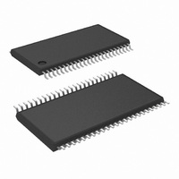
Physical Dimensions www.national.com inches (millimeters) unless otherwise noted Order Number DS90CR215MTD or DS90CR216MTD NS Package Number MTD48 16 ...
Page 17
Notes 17 www.national.com ...
Page 18
... For more National Semiconductor product information and proven design tools, visit the following Web sites at: Products Amplifiers www.national.com/amplifiers Audio www.national.com/audio Clock and Timing www.national.com/timing Data Converters www.national.com/adc Interface www.national.com/interface LVDS www.national.com/lvds Power Management www.national.com/power Switching Regulators www.national.com/switchers LDOs www.national.com/ldo LED Lighting www ...