DS90C385AMTX/NOPB National Semiconductor, DS90C385AMTX/NOPB Datasheet - Page 11
DS90C385AMTX/NOPB
Manufacturer Part Number
DS90C385AMTX/NOPB
Description
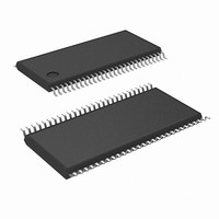
IC TX LVDS FPD 24BIT 56-TSSOP
Manufacturer
National Semiconductor
Type
Transmitterr
Datasheet
1.DS90C385AMTNOPB.pdf
(13 pages)
Specifications of DS90C385AMTX/NOPB
Number Of Drivers/receivers
1/0
Protocol
LVDS
Voltage - Supply
3 V ~ 3.6 V
Mounting Type
Surface Mount
Package / Case
56-TSSOP
Leaded Process Compatible
Yes
Rohs Compliant
Yes
Peak Reflow Compatible (260 C)
Yes
For Use With
FLINK3V8BT-85 - BOARD EVAL DS90C385A,DS90CF386
Lead Free Status / RoHS Status
Lead free / RoHS Compliant
Other names
DS90C385AMTX
Available stocks
Company
Part Number
Manufacturer
Quantity
Price
Company:

Part Number:
DS90C385AMTX/NOPB
Manufacturer:
NSC
Quantity:
130


Pin Diagram for TSSOP Packages
Applications Information
The
DS90C385, DS90C383A, DS90C383 in TSSOP 56-lead
package, and it is a pin-for-pin replacements.
This device DS90C385A also features reduced variation of
the TCCD parameter which is important for dual pixel appli-
cations. (See AN-1084)
This device may also be used as a replacement for the
DS90CF583 (5V, 65MHz) and DS90CF581 (5V, 40MHz)
FPD-Link
modifications:
1. Change 5V power supply to 3.3V. Provide this 3.3V
2. The DS90C385A transmitter input and control inputs
3. To implement a falling edge device for the DS90C385A,
TRANSMITTER INPUT PINS
The TxIN and control input pins are compatible with LVC-
MOS and LVTTL levels. These pins are not 5V tolerant.
TRANSMITTER INPUT CLOCK/DATA SEQUENCING
Unlike
DS90C385A does not require any special requirement for
sequencing of the input clock/data and PD (PowerDown)
signal. The DS90C385A offers a more robust input sequenc-
supply to the V
transmitter.
accept 3.3V LVTTL/LVCMOS levels. They are not 5V
tolerant.
the R_FB pin may be tied to ground OR left unconnected
(an internal pull-down resistor biases this pin low). Bias-
ing this pin to Vcc implements a rising edge device.
DS90C385A is
the
Transmitters
DS90C385,
CC
, LVDS V
backward
with
DS90C(F)383A/363A,
CC
certain
compatible
and PLL V
considerations/
CC
with
of the
DS90C385AMT
the
the
11
ing feature where the input clock/data can be inserted after
the release of the PD signal. In the case where the clock/
data is stopped and reapplied, such as changing video mode
within Graphics Controller, it is not necessary to cycle the PD
signal. However, there are in certain cases where the PD
may need to be asserted during these mode changes. In
cases where the source (Graphics Source) may be supply-
ing an unstable clock or spurious noisy clock output to the
LVDS transmitter, the LVDS Transmitter may attempt to lock
onto this unstable clock signal but is unable to do so due the
instability or quality of the clock source. The PD signal in
these cases should then be asserted once a stable clock is
applied to the LVDS transmitter. Asserting the PWR DOWN
pin will effectively place the device in reset and disable the
PLL, enabling the LVDS Transmitter into a power saving
standby mode. However, it is still generally a good practice
to assert the PWR DOWN pin or reset the LVDS transmitter
whenever the clock/data is stopped and reapplied but it is
not mandatory for the DS90C385A.
SPREAD SPECTRUM CLOCK SUPPORT
The DS90C385A can support Spread Spectrum Clocking
signal type inputs. The DS90C385A outputs will accurately
track Spread Spectrum Clock/Data inputs with modulation
frequencies of up to 100kHz (max.)with either center spread
of
POWER SOURCES SEQUENCE
In typical applications, it is recommended to have V
V
separate de-coupling bypass capacitor groups. There is no
requirement on which VCC entering the device first.
CC
±
2.5% or down spread -5% deviations.
and PLL V
20070223
CC
from the same power source with three
www.national.com
CC
, LVDS
Related parts for DS90C385AMTX/NOPB
Image
Part Number
Description
Manufacturer
Datasheet
Request
R

Part Number:
Description:
National Semiconductor [8-Bit D/A Converter]
Manufacturer:
National Semiconductor
Datasheet:
Part Number:
Description:
National Semiconductor [Media Coprocessor]
Manufacturer:
National Semiconductor
Datasheet:
Part Number:
Description:
Digitally Controlled Tone and Volume Circuit with Stereo Audio Power Amplifier, Microphone Preamp Stage and National 3D Sound
Manufacturer:
National Semiconductor
Datasheet:
Part Number:
Description:
Digitally Controlled Tone and Volume Circuit with Stereo Audio Power Amplifier, Microphone Preamp Stage and National 3D Sound
Manufacturer:
National Semiconductor
Datasheet:
Part Number:
Description:
AC97 Rev 2 Codec with Sample Rate Conversion and National 3D Sound
Manufacturer:
National Semiconductor
Part Number:
Description:
Manufacturer:
National Semiconductor
Datasheet:
Part Number:
Description:
Manufacturer:
National Semiconductor
Datasheet:
Part Number:
Description:
General Purpose, Low Voltage, Low Power, Rail-to-Rail Output Operational Amplifiers
Manufacturer:
National Semiconductor
Datasheet:
Part Number:
Description:
8-bit 20 MSPS flash A/D converter.
Manufacturer:
National Semiconductor
Datasheet:
Part Number:
Description:
Low Noise Quad Operational Amplifier
Manufacturer:
National Semiconductor
Datasheet:
Part Number:
Description:
Quad Differential Line Receivers
Manufacturer:
National Semiconductor
Datasheet:
Part Number:
Description:
Quad High Speed Trapezoidal? Bus Transceiver
Manufacturer:
National Semiconductor
Datasheet:
Part Number:
Description:
Dual Line Receiver
Manufacturer:
National Semiconductor
Datasheet:
Part Number:
Description:
TTL to 10k ECL Level Translator with Latch
Manufacturer:
National Semiconductor
Datasheet: