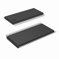
DS90C385AMTX/NOPB National Semiconductor, DS90C385AMTX/NOPB Datasheet - Page 4

DS90C385AMTX/NOPB
Manufacturer Part Number
DS90C385AMTX/NOPB
Description
IC TX LVDS FPD 24BIT 56-TSSOP
Manufacturer
National Semiconductor
Type
Transmitterr
Datasheet
1.DS90C385AMTNOPB.pdf
(13 pages)
Specifications of DS90C385AMTX/NOPB
Number Of Drivers/receivers
1/0
Protocol
LVDS
Voltage - Supply
3 V ~ 3.6 V
Mounting Type
Surface Mount
Package / Case
56-TSSOP
Leaded Process Compatible
Yes
Rohs Compliant
Yes
Peak Reflow Compatible (260 C)
Yes
For Use With
FLINK3V8BT-85 - BOARD EVAL DS90C385A,DS90CF386
Lead Free Status / RoHS Status
Lead free / RoHS Compliant
Other names
DS90C385AMTX
Available stocks
Company
Part Number
Manufacturer
Quantity
Price
Company:
Part Number:
DS90C385AMTX/NOPB
Manufacturer:
NSC
Quantity:
130
www.national.com
TPPos0
TPPos1
TPPos2
TPPos3
TPPos4
TPPos5
TPPos6
TPPos0
TPPos1
TPPos2
TPPos3
TPPos4
TPPos5
TPPos6
TPPos0
TPPos1
TPPos2
TPPos3
TPPos4
TPPos5
TPPos6
TSTC
THTC
TCCD
Transmitter Switching Characteristics
Over recommended operating supply and temperature ranges unless otherwise specified
Symbol
Transmitter Output Pulse Position (Figure 12)
(Note 5)
Transmitter Output Pulse Position
Transmitter Output Pulse Position
Transmitter Output Pulse Position
Transmitter Output Pulse Position
Transmitter Output Pulse Position
Transmitter Output Pulse Position
Transmitter Output Pulse Position (Figure 12)
(Note 5)
Transmitter Output Pulse Position
Transmitter Output Pulse Position for Bit 2
Transmitter Output Pulse Position for Bit 3
Transmitter Output Pulse Position
Transmitter Output Pulse Position
Transmitter Output Pulse Position
Transmitter Output Pulse Position (Figure 12)
(Note 5)
Transmitter Output Pulse Position
Transmitter Output Pulse Position
Transmitter Output Pulse Position
Transmitter Output Pulse Position
Transmitter Output Pulse Position
Transmitter Output Pulse Position
Required TxIN Setup to TxCLK IN
(Figure 6) at 85MHz
Required TxIN Hold to TxCLK IN (Figure 6) at
87.5 MHz
TxCLK IN to TxCLK OUT Delay. Measure from
TxCLK IN edge to immediately crossing point of
differential TxCLK OUT by following the positive
TxCLK OUT. 50% duty cycle input clock is
assumed. (Figure 7)
Measure from TxCLK IN edge to immediately
crossing point of differential TxCLK OUT by
following the positive TxCLK OUT. 50% duty
cycle input clock is assumed. (Figure 8)
Parameter
T
and 87.5MHz
for " Min ",
T
25MHz for "
Max ", V
3.6V, R_FB
pin = VCC
T
and 87.5MHz
for " Min ",
T
25MHz for "
Max ", V
3.6V, R_FB
pin = GND
4
f = 87.5 MHz
f = 40 MHz
f = 65 MHz
A
A
A
A
(Continued)
= −10˚,
= 70˚, and
= −10˚,
= 70˚, and
CC
CC
=
=
−0.25
10.46
14.04
17.61
21.18
−0.20
10.79
12.99
−0.20
3.086
2.868
3.32
6.89
2.00
4.20
6.39
8.59
1.48
3.16
4.84
6.52
8.20
9.88
Min
2.5
0.5
10.71
14.29
17.86
21.43
10.99
13.19
10.08
3.57
7.14
2.20
4.40
6.59
8.79
1.68
3.36
5.04
6.72
8.40
Typ
0
0
0
+0.25
10.96
14.54
18.11
21.68
+0.20
11.19
13.39
+0.20
10.28
7.211
6.062
Max
3.82
7.39
2.40
4.60
6.79
8.99
1.88
3.56
5.24
6.92
8.60
Units
ns
ns
ns
ns
ns
ns
ns
ns
ns
ns
ns
ns
ns
ns
ns
ns
ns
ns
ns
ns
ns
ns
ns
ns
ns


