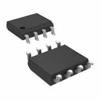
CLC005AJE-TR13/NOPB National Semiconductor, CLC005AJE-TR13/NOPB Datasheet - Page 6

CLC005AJE-TR13/NOPB
Manufacturer Part Number
CLC005AJE-TR13/NOPB
Description
IC CABLE DRIVER DGTL ADJ 8-SOIC
Manufacturer
National Semiconductor
Series
CLCr
Type
Driverr
Datasheet
1.CLC005AJENOPB.pdf
(12 pages)
Specifications of CLC005AJE-TR13/NOPB
Number Of Drivers/receivers
1/0
Voltage - Supply
4.5 V ~ 5.5 V
Mounting Type
Surface Mount
Package / Case
8-SOIC (3.9mm Width)
For Use With
SD005EVK - BOARD EVALUATION CLC005
Lead Free Status / RoHS Status
Lead free / RoHS Compliant
Protocol
-
Other names
*CLC005AJE-TR13
*CLC005AJE-TR13/NOPB
CLC005AJE-TR13
*CLC005AJE-TR13/NOPB
CLC005AJE-TR13
www.national.com
Operation
OUTPUT AMPLITUDE ADJUSTMENT
The high and low output levels of the CLC005 are set by a
circuit shown simplified in Figure 8 . Output high and low lev-
els may be set independently with external resistor networks
connected between R
power supplies. The resistor networks affect the high and
low output levels by changing the internally generated bias
voltages, V
are V
R
components which determine output voltage levels have ac-
curate ratios, their absolute values may be controlled only
within about
justment, output voltages are well controlled. A final design
should accommodate the variation in externally set output
voltages due to the CLC005’s part-to-part and external com-
ponent tolerances.
Output voltage swing may be reduced with the circuit shown
in Figure 9 . A single resistance chosen with the aid of the
graph, Figure 10 , is connected between pins 3 and 4. Output
voltage swing may be increased with the circuit of Figure 11 .
Figure 12 is used to estimate a value for resistor R. Note that
both of these circuits and the accompanying graphs assume
that the CLC005 is loaded with the standard 150 . Be aware
that output loading will affect the output swing and the high
EXT-H
CC
and R
−1.7V and V
H
±
and V
EXT-L
15% of nominal. Even so, without external ad-
(Continued)
are left unconnected. Though the internal
L
. The nominal high and low output levels
CC
EXT-H
−3.7V, respectively, when the pins
(pin 3), R
FIGURE 7. Differential Input DC Coupled Output
EXT-L
(pin 4) and the
6
and low levels. It may be necessary to empirically select re-
sistances used to set output levels when the D.C. loading on
the CLC005 differs appreciably from 150 .
FIGURE 8. Equivalent Bias Generation Circuit
DS100144-10
DS100144-11


