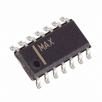
MAX13184EESD+ Maxim Integrated Products, MAX13184EESD+ Datasheet - Page 11

MAX13184EESD+
Manufacturer Part Number
MAX13184EESD+
Description
IC TXRX RS-485 +5.0V ESD 14SOIC
Manufacturer
Maxim Integrated Products
Type
Transceiverr
Datasheet
1.MAX13182EELBT.pdf
(18 pages)
Specifications of MAX13184EESD+
Number Of Drivers/receivers
1/1
Protocol
RS485
Voltage - Supply
4.5 V ~ 5.5 V
Mounting Type
Surface Mount
Package / Case
14-SOIC (3.9mm Width), 14-SOL
Lead Free Status / RoHS Status
Lead free / RoHS Compliant
The MAX13181E–MAX13184E high-speed transceivers
for RS-485 communication contain one driver and one
receiver. These devices feature 1/8 unit-load input
impedance that allows up to 256 receivers on the bus.
All devices feature integrated pullup/pulldown resistors
on the DE, RE, and H/F inputs to reduce external com-
ponents. The MAX13182E/MAX13184E feature a low-
current shutdown mode for power-sensitive applications.
The MAX13181E/MAX13182E feature reduced slew-rate
drivers to minimize EMI and reflections that are caused
by improperly terminated cables. The slew-rate limited
MAX13181E/MAX13182E allow error-free transmission
up to 250Kbps. The MAX13183E/MAX13184E feature
full-speed drivers allowing data rate of up to 16Mbps.
The MAX13182E/MAX13184E are configured for full-
duplex operation. The MAX13181E/MAX13183E feature
selectable half- or full-duplex operation by driving H/F
input high or low, respectively. All devices operate from
a single +5.0V supply.
MAX13181E/
MAX13183E
10
—
—
1
2
3
4
5
6
7
8
9
µDFN
MAX13182E/
MAX13184E
+5.0V, ±15kV ESD-Protected, Half-Duplex/
______________________________________________________________________________________
Full-Duplex, RS-485 Transceiver in µDFN
10
—
—
1
2
3
4
5
6
7
8
9
Detailed Description
MAX13182E/
MAX13184E
1, 8, 13
6, 7
SO
14
10
11
12
—
2
3
4
5
9
NAME
GND
N.C.
V
H/F
RO
DE
RE
DI
B
A
CC
Y
Z
Positive Supply, V
capacitor to ground.
Receiver Output. When RE is low and (A-B) ≥ 200mV, RO is high; if (A-B) ≤
-200mV, RO is low.
Receiver Output Enable. Drive RE low to enable RO. Drive RE high to
disable the receiver. RE input has an internal pullup resistor.
Half-/Full-Duplex Selector Input. Connect H/F to V
Leave H/F unconnected or connect H/F to GND for full-duplex mode. H/F
input has an internal pulldown resistor.
D r i ver O utp ut E nab l e. D r i ve D E hi g h to enab l e the d r i ver . D r i ver outp ut i s hi g h
i m p ed ance w hen D E i s l ow . D E i np ut has an i nter nal p ul l d ow n r esi stor .
Driver Input. With DE high, a low on DI forces noninverting output low and
inverting output high. Similarly, a high on DI forces noninverting output high
and inverting output low.
Ground
Noninverting Driver Output. (Also noninverting receiver input in half-duplex
mode.)
Inver ti ng D r i ver Outp ut. ( Al so i nver ti ng r ecei ver i np ut i n hal f- d up l ex m od e.)
Inverting Receiver Input
Noninverting Receiver Input
No Connection. N.C. is not internally connected.
As with all Maxim devices, ESD-protection structures
are incorporated on all pins to protect against electro-
static discharges encountered during handling and
assembly. The driver outputs of the MAX13181E–
MAX13184E family have extra protection against static
electricity. Maxim’s engineers have developed state-of-
the-art structures to protect these driver outputs against
ESD of ±15kV with V
logic state of DE and DI.
The ESD-protected pins are tested with reference to the
ground pin in a powered-down condition. They are test-
ed to ±15kV using the Human Body Model, ±12kV using
the IEC 61000-4-2 Air-Gap Discharge Model, and to
±6kV using the IEC 61000-4-2 Contact Discharge Model.
ESD performance depends on a variety of conditions.
Contact Maxim for a reliability report that documents
test setup, test methodology, and test results.
CC
= +4.5V to +5.5V. Bypass V
FUNCTION
CC
= 5V, and regardless of the
±15kV ESD Protection
Pin Description
CC
CC
ESD Test Conditions
with a 0.1µF ceramic
for half-duplex mode.
11


