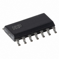
TJA1041AT/N,112 NXP Semiconductors, TJA1041AT/N,112 Datasheet - Page 10

TJA1041AT/N,112
Manufacturer Part Number
TJA1041AT/N,112
Description
IC TXRX CAN 14BIT 27V SOT108-1
Manufacturer
NXP Semiconductors
Type
Transceiverr
Datasheet
1.TJA1041ATVM518.pdf
(25 pages)
Specifications of TJA1041AT/N,112
Number Of Drivers/receivers
1/1
Protocol
CAN
Voltage - Supply
4.75 V ~ 5.25 V
Mounting Type
Surface Mount
Package / Case
14-SOIC (3.9mm Width), 14-SOL
Lead Free Status / RoHS Status
Lead free / RoHS Compliant
Other names
935277288112
TJA1041AT/N
TJA1041AT/N
TJA1041AT/N
TJA1041AT/N
NXP Semiconductors
TJA1041A_4
Product data sheet
7.3.3 TXD-to-RXD short-circuit detection
7.3.4 Bus dominant clamping detection
7.3.5 Overtemperature detection
7.4 Recessive bus voltage stabilization
7.5 I/O level adapter
7.6 Pin WAKE
A short circuit between pins RXD and TXD would keep the bus in a permanent dominant
state once the bus is driven dominant, because the low-side driver of RXD is typically
stronger than the high-side driver of the controller connected to TXD. The TXD-to-RXD
short circuit detection prevents such a network lockup by disabling the transmitter. The
transmitter remains disabled until the local failure flag is cleared.
A CAN bus short circuit (to V
nodes could result in a differential voltage on the bus high enough to represent a bus
dominant state. Because a node will not start transmission if the bus is dominant, the
normal bus failure detection will not detect this failure, but the bus dominant clamping
detection will. The local failure flag is set if the dominant state on the bus persists for
longer than t
blocking network communication. There is no need to disable the transmitter. Note that
the local failure flag does not retain a bus dominant clamping failure and is released as
soon as the bus returns to recessive state.
To protect the output drivers of the transceiver against overheating, the transmitter will be
disabled if the virtual junction temperature exceeds the shutdown junction temperature
T
In recessive state the output impedance of transceivers is relatively high. In a partially
powered network (supply voltage is off in some of the nodes) any deactivated transceiver
with a significant leakage current is likely to load the recessive bus to ground. This will
cause a common-mode voltage step each time transmission starts, resulting in increased
EME. Using pin SPLIT of the TJA1041A in combination with split termination (see
Figure
pin SPLIT provides a stabilized 0.5V
command mode and Sleep mode pin SPLIT is set floating.
The TJA1041A is equipped with a built-in I/O-level adapter. By using the supply voltage of
the controller (to be supplied at pin V
I/O-levels of the transceiver. For pins TXD, STB and EN the digital input threshold level is
adjusted, and for pins RXD and ERR the HIGH-level output voltage is adjusted. This
allows the transceiver to be directly interfaced with controllers on supply voltages between
2.8 V and 5.25 V, without the need for glue logic.
Pin WAKE of the TJA1041A allows local wake-up triggering by a LOW-to-HIGH state
change as well as a HIGH-to-LOW state change. This gives maximum flexibility when
designing a local wake-up circuit. To keep current consumption at a minimum, after a t
delay the internal bias voltage of pin WAKE will follow the logic state of this pin. A HIGH
level on pin WAKE is followed by an internal pull-up to V
j(sd)
. The transmitter remains disabled until the local failure flag is cleared.
5) will reduce this step effect. In Normal mode and Pwon/Listen-only mode
dom(bus)
. By checking this flag, the controller can determine if a clamped bus is
Rev. 04 — 29 July 2008
BAT
, V
CC
CC
I/O
or GND) or a failure in one of the other network
) the level adapter ratiometrically scales the
DC voltage. In Standby mode, Go-to-sleep
BAT
High-speed CAN transceiver
. A LOW level on pin WAKE is
TJA1041A
© NXP B.V. 2008. All rights reserved.
10 of 25
wake


