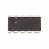
DS90CR281MTDX National Semiconductor, DS90CR281MTDX Datasheet

DS90CR281MTDX
Specifications of DS90CR281MTDX
Related parts for DS90CR281MTDX
DS90CR281MTDX Summary of contents
Page 1
... DS90CR281 Order Number DS90CR281MTD See NS Package Number MTD56 TRI-STATE ® registered trademark of National Semiconductor Corporation. © 1998 National Semiconductor Corporation DS012638 ground) are needed. This provides a 80% reduction in re- quired cable width, which provides a system cost savings, reduces connector physical size and cost, and reduces shielding requirements due to the cables’ ...
Page 2
Connection Diagrams DS90CR281 Typical Application www.national.com DS012638-2 2 DS90CR282 DS012638-3 DS012638-19 ...
Page 3
... Absolute Maximum Ratings If Military/Aerospace specified devices are required, please contact the National Semiconductor Sales Office/ Distributors for availability and specifications. Supply Voltage ( CMOS/TTL Input Voltage −0. CMOS/TTL Ouput Voltage −0. LVDS Receiver Input Voltage −0. LVDS Driver Output Voltage −0. LVDS Output Short Circuit ...
Page 4
Electrical Characteristics Over recommended operating supply and temperature ranges unless otherwise specified Symbol Parameter RECEIVER SUPPLY CURRENT I Receiver Supply Current, CCRW Worst Case I Receiver Supply Current, CCRZ Power Down Note 1: “Absolute Maximum Ratings” are those values beyond ...
Page 5
Receiver Switching Characteristics Over recommended operating supply and temperature ranges unless otherwise specified Symbol CLHT CMOS/TTL Low-to-High Transition Time ( Figure 3 ) CMOS/TTL High-to-Low Transition Time ( Figure 3 ) CHLT RCOP RxCLK OUT Period ( Figure 7 ) ...
Page 6
AC Timing Diagrams (Continued) DS012638-7 FIGURE 3. DS90CR282 (Receiver) CMOS/TTL Output Load and Transition Timing FIGURE 4. DS90CR281 (Transmitter) Input Clock Transition Time = 0V Measurements at V diff = 0V Measurements at V diff TCCS measured between earliest and ...
Page 7
AC Timing Diagrams (Continued) FIGURE 7. (Receiver) DS90CR282 Setup/Hold and High/Low Times FIGURE 8. DS90CR281 (Transmitter) Clock In to Clock Out Delay FIGURE 9. DS90CR282 (Receiver) Clock In to Clock Out Delay FIGURE 10. DS90CR281 (Transmitter) Phase Lock Loop Set ...
Page 8
AC Timing Diagrams (Continued) FIGURE 11. DS90CR282 (Receiver) Phase Lock Loop Set Time FIGURE 12. Seven Bits of LVDS in One Clock Cycle FIGURE 13. 28 Parallel TTL Data Inputs Mapped to LVDS Outputs (DS90CR281) www.national.com FIGURE 14. Transmitter Powerdown ...
Page 9
AC Timing Diagrams (Continued) FIGURE 15. Receiver Powerdown Delay FIGURE 16. Transmitter LVDS Output Pulse Position Measurement SW — Setup and Hold Time (Internal data sampling window) TCCS — Transmitter Output Skew RSKM Cable Skew (type, length) + Source Clock ...
Page 10
DS90CR281 Pin Description — Channel Link Transmitter (Tx) Pin Name I/O No. TxIN I 28 TTL Level inputs TxOUT Positive LVDS differential data output TxOUT− Negative LVDS differential data output TxCLK TTL level ...
Page 11
Applications Information (Continued) is good for short and long applications. When using ribbon cable recommended to place a ground line between each differential pair to act as a barrier to noise coupling be- tween adjacent pairs. For Twin-Coax ...
Page 12
Applications Information FIGURE 19. CHANNEL LINK Decoupling Configuration CLOCK JITTER: The CHANNEL LINK devices employ a PLL to generate and recover the clock transmitted across the LVDS interface. The width of each bit in the serialized LVDS data stream is ...
Page 13
13 ...
Page 14
... National Semiconductor Asia Pacific Customer Fax: +49 (0) 1 80-530 85 86 Response Group Email: europe.support@nsc.com Tel: 65-2544466 Fax: 65-2504466 Tel: +49 (0) 1 80-532 78 32 Email: sea.support@nsc.com Tel: +49 (0) 1 80-534 16 80 National Semiconductor Japan Ltd. Tel: 81-3-5620-6175 Fax: 81-3-5620-6179 ...


