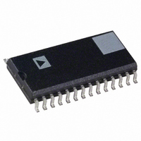
AD1892JRRL Analog Devices Inc, AD1892JRRL Datasheet - Page 18

AD1892JRRL
Manufacturer Part Number
AD1892JRRL
Description
IC SAMPLE CONV W/RX 20BIT 28SOIC
Manufacturer
Analog Devices Inc
Type
Sample Rate Converterr
Datasheet
1.AD1892JR.pdf
(24 pages)
Specifications of AD1892JRRL
Rohs Status
RoHS non-compliant
Applications
Players, Recorders
Voltage - Supply, Digital
4.5 V ~ 5.5 V
Mounting Type
Surface Mount
Package / Case
28-SOIC (7.5mm Width)
Voltage - Supply, Analog
-
AD1892
Note that in 16-bit output mode, the AD1892 is capable of a
32
left-justified to an LRCLK transition, and the LSB is right-
justified to an LRCLK transition. LRCLK is HI for the left
channel and LO for the right channel. Data is valid on the
rising edge of BCLK. Packed mode can be used when the
AD1892 is programmed in either right-justified or left-justified
mode. Packed mode is shown in Figure 30.
ASRC Bypass Mode
By setting bit D0 HI in Control Register 1, the AD1892 will be
placed in “bypass mode,” where the received biphase-mark
encoded data is transmitted out of serial output interface with-
out any sample rate conversion applied. This mode may be
useful in applications where the audio data is not simple PCM
information; for example, the data may be compressed using the
MPEG or Dolby AC-3 compression standards. In this mode, the
output interface runs in master mode (LRCLK and BCLK are
outputs), and all three output format modes are available (left-
justified, I
out an external PLL, jitter may be as high as one MCLK period.
In bypass mode, the output sample frequency (LRCLK fre-
quency) is simply the incoming biphase-mark sample frequency.
The BCLK frequency can be set to 32
(default) using Bit D1 in Control Register 1.
Power-Down and Reset
The AD1892 offers two methods of initiating power-down/reset:
through an input pin (PD/RST, Pin 1) and through a control
register bit (Control Register 0, Bit D0). When the PD/RST pin
is held low, the AD1892 is placed in a “hardware” low dissipa-
tion power-down state with the on-chip clocks stopped. When
the PD/RST input is asserted HI, the AD1892 is reset. The two
control registers in the serial control port are initialized to their
default values. All other on-chip registers are zeroed, including
those in the rate converter, the serial data output port, the status
registers, the Channel Status, and Q-Channel subcode registers.
The AD1892 enters the default mode and is ready for normal
operation. The master clock (MCLK, Pin 28) must be running
for a successful hardware reset or power-down operation to occur.
The PD/RST signal must be LO for a minimum of four master
clock periods ( 160 ns with a 24.576 MHz MCLK frequency).
“Software” power-down is activated by writing 1 to bit D0 in
Control Register 0. The effect is the same as hardware power-
down/reset, except the clocks to the SPI serial control port are
not stopped, so that the AD1892 may be put back into normal
operation.
F
SOUT
2
S-justified and right-justified). In bypass mode, with-
BCLK frequency “packed mode” where the MSB is
OUTPUT
OUTPUT
OUTPUT
SDATA
LRCLK
BCLK
LSB
MSB
MSB–1 MSB–2
LEFT CHANNEL
F
SIN
or 64
Figure 30. 32
F
LSB+2 LSB+1
SIN
–18–
LSB
F
S
Multiple AD1892 Synchronization
Two methods can be used to synchronize the outputs of mul-
tiple AD1892s.
It is possible to synchronize the outputs of multiple AD1892s in
a system by issuing them PD/RST signals which are synchronous
with the MCLK signal. This scheme is illustrated in Figure 31.
The second method involves using the SYNC input. A falling
edge on the SYNC input resets output timing counters within
the AD1892. See Figure 41 for timing. Note that the SYNC
signal MUST be divided down from the 512 F
signal applied to the AD1892. If SYNC is properly set up to
MCLK, the current LRCLK and BCLK timing will be inter-
rupted, and the left/right channel sample pair will be invalid.
However, the second and subsequent left/right sample pairs will
have valid data and normally timed bit and left/right clocks. If
the AD1892 is configured for a 64
(default), the LRCLK output (on the second and subsequent
output periods) will fall immediately after SYNC falls (i.e., on
the next MCLK falling edge). The SYNC input to the AD1892
can be used externally as the system LRCLK clock (or word
clock) when the AD1892 is configured in 64 F
mode. When the AD1892 is configured in 32
mode, LRCLK falls several MCLK falling edges later, and the
SYNC input cannot be used as the external LRCLK signal
directly. Note that Figure 41 shows the 64 F
mode only. Figure 32 shows several AD1892s synchronized
using the SYNC input. SYNC input synchronization is not
available when the AD1892 is used in bypass mode.
MSB
Packed Mode
RIGHT CHANNEL
MSB–1 MSB–2
Figure 31. Multiple AD1892 Synchronization
AD1892
AD1892
AD1892
PD/RST
PD/RST
PD/RST
MCLK
MCLK
MCLK
LSB+2 LSB+1
28
28
28
1
1
1
LSB
MSB
Q
F
SOUT
MSB+1
D
bit clock frequency
ASYNCHRONOUS
RESET
512 x F
SOUT
F
SOUT
SOUT
SOUT
SOUT
bit clock
bit clock
MCLK
bit clock
REV. 0


