MPR121QR2 Freescale Semiconductor, MPR121QR2 Datasheet - Page 8
MPR121QR2
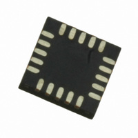
Manufacturer Part Number
MPR121QR2
Description
IC CTLR TOUCH SENSOR 20-QFN
Manufacturer
Freescale Semiconductor
Type
Capacitive, Proximity Sensorr
Datasheet
1.MPR121QR2.pdf
(57 pages)
Specifications of MPR121QR2
Number Of Inputs/keys
12 Key
Data Interface
I²C, Serial
Voltage - Supply
1.71 V ~ 3.6 V
Current - Supply
29µA
Operating Temperature
-40°C ~ 85°C
Mounting Type
Surface Mount
Package / Case
20-UQFN, 20-µQFN
Output Type
Logic
Interface
I²C
Input Type
Logic
Supply Voltage
2.5 V to 3.6 V
Dimensions
3 mm L x 3 mm W x 0.65 mm H
Temperature Range
- 40 C to + 85 C
Termination Style
SMD/SMT
Supply Current
29µA
Ic Interface Type
I2C
Supply Voltage Range
1.71V To 3.6V
Sensor Case Style
QFN
No. Of Pins
20
Operating Temperature Range
-40°C To +85°C
Interface Type
I2C
Rohs Compliant
Yes
Lead Free Status / RoHS Status
Lead free / RoHS Compliant
Other names
MPR121QR2
MPR121QR2TR
MPR121QR2TR
Available stocks
Company
Part Number
Manufacturer
Quantity
Price

Part Number:
MPR121QR2
Manufacturer:
FREESCALE
Quantity:
20 000


Table 3. ESD and Latch-up Test Conditions
MPR121
8
ELECTRICAL CHARACTERISTICS
Absolute Maximum Ratings
Absolute maximum ratings are stress ratings only, and functional operation at the maxima is not guaranteed. Stress beyond the
limits specified in
conditions, refer to the remaining tables in this section. This device contains circuitry protecting against damage due to high static
voltage or electrical fields; however, it is advised that normal precautions be taken to avoid application of any voltages higher
than maximum-rated voltages to this high-impedance circuit.
ESD AND LATCH-UP PROTECTION CHARACTERISTICS
Normal handling precautions should be used to avoid exposure to static discharge.
Qualification tests are performed to ensure that these devices can withstand exposure to reasonable levels of static without
suffering any permanent damage. During the device qualification ESD stresses were performed for the Human Body Model
(HBM), the Machine Model (MM) and the Charge Device Model (CDM).
A device is defined as a failure if after exposure to ESD pulses the device no longer meets the device specification. Complete
DC parametric and functional testing is performed per the applicable device specification at room temperature followed by hot
temperature, unless specified otherwise in the device specification.
Table 2. Absolute Maximum Ratings - Voltage (with respect to V
Human Body Model (HBM)
Machine Model (MM)
Charge Device Model (CDM)
Latch-up current at T
Supply Voltage
Supply Voltage
Input Voltage
Operating Temperature Range
GPIO Source Current per Pin
GPIO Sink Current per Pin
Storage Temperature Range
SCL, SDA, IRQ
Table 2
A
Rating
= 85°C
Rating
may affect device reliability or cause permanent damage to the device. For functional operating
Symbol
V
i
i
V
GPIO
GPIO
V
T
T
REG
DD
IN
O
S
Symbol
I
V
V
V
LATCH
ESD
ESD
ESD
SS
)
V
SS
- 0.3 to V
-0.3 to +2.75
-0.3 to +3.6
-40 to +125
-40 to +85
Value
1.2
12
±2000
Value
±200
±500
±100
DD
+ 0.3
Freescale Semiconductor
Unit
mA
Unit
V
V
V
mA
mA
°C
°C
V
V
V
Sensors
Related parts for MPR121QR2
Image
Part Number
Description
Manufacturer
Datasheet
Request
R

Part Number:
Description:
Proximity Capacitive Touch Sensor Controller
Manufacturer:
FREESCALE [Freescale Semiconductor, Inc]
Datasheet:

Part Number:
Description:
Manufacturer:
Freescale Semiconductor, Inc
Datasheet:
Part Number:
Description:
Manufacturer:
Freescale Semiconductor, Inc
Datasheet:
Part Number:
Description:
Manufacturer:
Freescale Semiconductor, Inc
Datasheet:
Part Number:
Description:
Manufacturer:
Freescale Semiconductor, Inc
Datasheet:
Part Number:
Description:
Manufacturer:
Freescale Semiconductor, Inc
Datasheet:
Part Number:
Description:
Manufacturer:
Freescale Semiconductor, Inc
Datasheet:
Part Number:
Description:
Manufacturer:
Freescale Semiconductor, Inc
Datasheet:
Part Number:
Description:
Manufacturer:
Freescale Semiconductor, Inc
Datasheet:
Part Number:
Description:
Manufacturer:
Freescale Semiconductor, Inc
Datasheet:
Part Number:
Description:
Manufacturer:
Freescale Semiconductor, Inc
Datasheet:
Part Number:
Description:
Manufacturer:
Freescale Semiconductor, Inc
Datasheet:
Part Number:
Description:
Manufacturer:
Freescale Semiconductor, Inc
Datasheet:
Part Number:
Description:
Manufacturer:
Freescale Semiconductor, Inc
Datasheet:
Part Number:
Description:
Manufacturer:
Freescale Semiconductor, Inc
Datasheet: