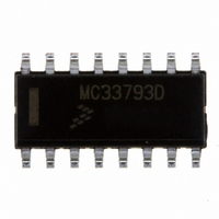
MC33793DR2 Freescale Semiconductor, MC33793DR2 Datasheet - Page 19

MC33793DR2
Manufacturer Part Number
MC33793DR2
Description
IC DSI SLAVE FOR R-SENSE 16-SOIC
Manufacturer
Freescale Semiconductor
Type
Distributed Systems Interfacer
Datasheet
1.MCZ33793EFR2.pdf
(27 pages)
Specifications of MC33793DR2
Input Type
Logic
Output Type
Logic
Interface
2 Line, I²C (CLK, Address/Data)
Mounting Type
Surface Mount
Package / Case
16-SOIC (3.9mm Width)
Lead Free Status / RoHS Status
Contains lead / RoHS non-compliant
Current - Supply
-
Lead Free Status / Rohs Status
Not Compliant
Other names
MC33793DR2TR
device address register on the next and all subsequent
power-ups. If the device is not blank, this command will return
the programmed value during the next message time.
ensures that the device always acts as a dynamically
Table 21. Read/Write NVM Command Format
READ/WRITE NVM RESPONSE
following a valid Read/Write NVM command to the addressed
Table 22. Read/Write NVM Response Format
CLEAR LOGIC OUT COMMAND
logic low. The compliment to this command is the Set Logic
Table 23. Clear Logic Out Command Format
CLEAR LOGIC OUT RESPONSE
following a valid Clear Logic Out command to the addressed
Table 24. Clear Logic Out Response Format
Analog Integrated Circuit Device Data
Freescale Semiconductor
Legend
A[3:0] = Address bits. These bits are the address of the device
previously sent with the Initialization command. They must match
the address in the PA[3:0] field and the address stored in the
device address register.
Legend
A[3:0] = Address bits. The slave address.
PA[3:0] = Programmed Address bits. The address that was
programmed into the NVM address bits of the slave.
Legend
A[3:0] = Address bits. The address of the selected device.
Legend
A[3:0] = Address bits. The slave address.
BS = Bus Switch Position (1=closed).
LO = Logic out driven level.
IO[3:0] = Values at logic I/Os.
A3
A3
1
–
Programming the NVM address to $0 is allowed. This
This response message is sent during the next message
The Clear Logic Out command sets the Logic Out pin to a
This response message is sent during the next message
A2
A2
1
–
A1
1
A1
–
High Byte
High Byte
A0
1
A0
–
Data
Data
0
PA3
0
–
0
0
PA2
–
0
0
–
PA1
0
0
–-
PA0
NV
1
A3
A3
1
U
X[3:0] = Cyclic Redundancy Check (CRC). The CRC as calculated by the
master.
A2
Address
X[3:0] = Cyclic Redundancy Check (CRC). The CRC as calculated by the
slave.
PA[3:0] = Program Address bits. These bits are the address that is to be
programmed into the slave.
X[3:0] = Cyclic Redundancy Check (CRC). The CRC as calculated by the
master.
A2
1
Address
NV = Nonvolatile Memory Write. The value of the NV bit in the slave.
U = Undervoltage indicated true by a “1”.
X[3:0] = Cyclic Redundancy Check (CRC). The CRC as calculated by the
slave.
LO
A1
addressable device and would be immune to any inadvertent
future NVM programming sequences.
command format is found in
device. The response format is found in
byte is omitted during the short-word response. No response
is generated if the command address field was $0.
Out. The Logic Out is also cleared at power-up or following a
Clear command. The format of the Clear Logic Out command
is shown in
device. The response is shown in
generated if the command address field was $0.
1
A1
Reads and writes are long-word commands only. The
Low Byte
Low Byte
BS
A0
PA3
A0
IO3
Table
1
PA2
1
Command
IO2
23.
Command
1
0
PA1
IO1
0
DSI COMMANDS AND RESPONSES
0
FUNCTIONAL DEVICE OPERATION
Table
PA0
IO0
0
1
Table
21.
X3
X3
X3
X3
Table
24. No response is
X2
X2
X2
X2
CRC
CRC
CRC
CRC
22. The high
X1
X1
X1
X1
33793
X0
X0
X0
X0
19


