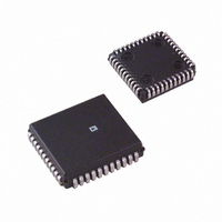
AD2S83IP-REEL Analog Devices Inc, AD2S83IP-REEL Datasheet - Page 12

AD2S83IP-REEL
Manufacturer Part Number
AD2S83IP-REEL
Description
IC R/D CONV TRACKING 44PLCC T/R
Manufacturer
Analog Devices Inc
Type
R/D Converterr
Datasheet
1.AD2S83IPZ-REEL.pdf
(19 pages)
Specifications of AD2S83IP-REEL
Rohs Status
RoHS non-compliant
Input Type
Parallel
Output Type
Digital
Interface
Parallel
Current - Supply
30mA
Mounting Type
Surface Mount
Package / Case
44-PLCC
AD2S83
Ratio Multiplier
The ratio multiplier is the input section of the AD2S83. This
compares the signal from the resolver (angle θ) to the digital
(angle φ) held in the counter. Any difference between these
two angles results in an analog voltage at the AC ERROR
OUTPUT. This circuit function has historically been called a
“Control Transformer” as it was originally performed by an
electromechanical device known by that name.
The AC ERROR signal is given by
where ω = 2 π f
So for 2 V rms inputs signals
AC ERROR output in volts/(bit of error)
where n = bits per rev
giving an AC ERROR output
The ratio multiplier will work in exactly the same way whether
the AD2S83 is connected as a tracking converter or as a control
transformer, where data is preset into the counters using the
DATA LOAD pin.
HF Filter
The AC ERROR OUTPUT may be fed to the PSD via a simple
ac coupling network (R2, C1) to remove any dc offset at this
point. Note, however, that the PSD of the AD2S83 is a wide-
band demodulator and is capable of aliasing HF noise down to
within the loop bandwidth. This is most likely to happen where
the resolver is situated in particularly noisy environments, and
the user is advised to fit a simple HF filter R1, C2 prior to the
phase sensitive demodulator.
The attenuation and frequency response of a filter will affect the
loop gain and must be taken into account in deriving the loop
transfer function. The suggested filter (R1, C1, R2, C2) is
shown in Figure 1 and gives an attenuation at the reference
frequency (f
demodulator.
Values of components used in the filter must be chosen to
ensure that the phase shift at f
to reference phase shift of the converter.
f
A1 = the gain of the ratio multiplier stage = 14.5.
REF
= reference frequency
= 1,024 for 10-bit resolution
= 4,096 for 12-bit resolution
= 16,384 for 14-bit resolution
= 65,536 for 16-bit resolution
= 178 mV/bit @ 10-bit resolution
= 44.5 mV/bit @ 12-bit resolution
= 11.125 mV/bit @ 14-bit resolution
= 2.78 mV/bit @ 16-bit resolution
REF
REF
) of three times at the input to the phase sensitive
= 2 × sin
A1 sin (θ–φ) sin ω t
REF
360
n
is within the allowable signal
× A1
Phase Sensitive Demodulator
The phase sensitive demodulator is effectively ideal and devel-
ops a mean dc output at the DEMODULATOR OUTPUT
pin of
for sinusoidal signals in phase or antiphase with the reference
(for a square wave the DEMODULATOR OUTPUT voltage
will equal the DEMODULATOR INPUT). This provides a
signal at the DEMODULATOR OUTPUT which is a dc level
proportional to the positional error of the converter.
DC Error Scaling = 160 mV/bit (10-bit resolution)
When the tracking loop is closed, this error is nulled to zero
unless the converter input angle is accelerating.
Integrator
The integrator components (R4, C4, R5, C5) are external to the
AD2S83 to allow the user to determine the optimum dynamic
characteristics for any given application. The Component
Selection section explains how to select components for a
chosen bandwidth.
Since the output from the integrator is fed to the VCO INPUT,
it is proportional to velocity (rate of change of output angle) and
can be scaled by selection of R6, the VCO input resistor. This is
explained in the Voltage Controlled Oscillator (VCO) section
below.
To prevent the converter from “flickering” (i.e., continually
toggling by ± 1 bit when the quantized digital angle, φ, is not an
exact representation of the input angle, θ) feedback is internally
applied from the VCO to the integrator input to ensure that the
VCO will only update the counter when the error is greater than
or equal to 1 LSB. In order to ensure that this feedback “hys-
teresis” is set to 1 LSB the input current to the integrator must
be scaled to be 100 nA/bit. Therefore,
Any offset at the input of the integrator will affect the accuracy
of the conversion as it will be treated as an error signal and
offset the digital output. One LSB of extra error will be added
for each 100 nA of input bias current. The method of adjusting
out this offset is given in the Component Selection section.
Voltage Controlled Oscillator
The VCO is essentially a simple integrator feeding a pair of dc
level comparators. Whenever the integrator output reaches one
of the comparator threshold voltages, a fixed charge is injected
into the integrator input to balance the input current. At the
same time the counter is clocking either up or down, dependent
on the polarity of the input current. In this way the counter is
clocked at a rate proportional to the magnitude of the input
current of the VCO.
±2 2
π
× (DEMODULATOR INPUT rms voltage )
R4 =
= 40 mV/bit (12-bit resolution)
= 10 mV/bit (14-bit resolution)
= 2.5 mV/bit (16-bit resolution)
DC Error Scaling (mV /bit )
100 (nA /bit )
(VCO)


