AD2S83IP-REEL Analog Devices Inc, AD2S83IP-REEL Datasheet - Page 5
AD2S83IP-REEL
Manufacturer Part Number
AD2S83IP-REEL
Description
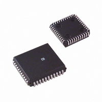
IC R/D CONV TRACKING 44PLCC T/R
Manufacturer
Analog Devices Inc
Type
R/D Converterr
Datasheet
1.AD2S83IPZ-REEL.pdf
(19 pages)
Specifications of AD2S83IP-REEL
Rohs Status
RoHS non-compliant
Input Type
Parallel
Output Type
Digital
Interface
Parallel
Current - Supply
30mA
Mounting Type
Surface Mount
Package / Case
44-PLCC


CAUTION
ESD (electrostatic discharge) sensitive device. Electrostatic charges as high as 4000 V readily
accumulate on the human body and test equipment and can discharge without detection. Although
the AD2S83 feature proprietary ESD protection circuitry, permanent damage may occur on devices
subjected to high-energy electrostatic discharges. Therefore, proper ESD precautions are
recommended to avoid performance degradation or loss of functionality.
ABSOLUTE MAXIMUM RATINGS
+V
–V
+V
Reference . . . . . . . . . . . . . . . . . . . . . . . . . . . . . . . +13 V to –V
SIN . . . . . . . . . . . . . . . . . . . . . . . . . . . . . . . . . . . +13 V to –V
COS . . . . . . . . . . . . . . . . . . . . . . . . . . . . . . . . . . +13 V to –V
Any Logical Input . . . . . . . . . . . . . . . . . . –0.4 V dc to +V
Demodulator Input . . . . . . . . . . . . . . . . . . . . . . . +13 V to –V
Integrator Input . . . . . . . . . . . . . . . . . . . . . . . . . . +13 V to –V
VCO Input . . . . . . . . . . . . . . . . . . . . . . . . . . . . . +13 V to –V
Power Dissipation . . . . . . . . . . . . . . . . . . . . . . . . . . . 800 mW
Operating Temperature
Storage Temperature . . . . . . . . . . . . . . . . . . –65°C to +150°C
Lead Temperature (Soldering, 10 sec) . . . . . . . . . . . . . 300°C
CAUTION
1
2
RECOMMENDED OPERATING CONDITIONS
Power Supply Voltage (+V
Power Supply Voltage V
Analog Input Voltage (SIN and COS) . . . . . . . 2 V rms ± 10%
Analog Input Voltage (REF) . . . . . . . . . . . . . . 1 V to 8 V peak
Signal and Reference Harmonic Distortion . . . . . . 10% (max)
Phase Shift Between Signal and Reference . . . ±10 Degrees (max)
Ambient Operating Temperature Range
Absolute Maximum Ratings are those values beyond which damage to the device
Correct polarity voltages must be maintained on the +V
may occur.
Industrial (AP, IP) . . . . . . . . . . . . . . . . . . . –40°C to +85°C
Industrial (AP, IP) . . . . . . . . . . . . . . . . . . . –40°C to +85°C
S
S
L
2
2
(MSB) DB1
NC = NO CONNECT
. . . . . . . . . . . . . . . . . . . . . . . . . . . . . . . . . . . . . . . . . . +V
. . . . . . . . . . . . . . . . . . . . . . . . . . . . . . . . . . . . . +13 V dc
. . . . . . . . . . . . . . . . . . . . . . . . . . . . . . . . . . . . . –13 V dc
SIN I/P
DB5
DB6
DB7
DB8
DB2
DB3
DB4
+V
NC
S
10
12
14
15
16
11
13
17
9
7
8
18 19 20 21 22 23 24 25 26 27 28
6
PIN CONFIGURATION
5
4
L
. . . . . . . . . . . . . . . . . +5 V dc ± 10%
3
S
(Not to Scale)
, –V
TOP VIEW
2
AD2S83
S
1 44
) . . . . . . . . . . ± 12 V dc ± 5%
PIN 1
IDENTIFIER
43
1
(with respect to GND)
42 41 40
S
and –V
39
38
37
36
35
34
33
32
31
30
29
S
pins.
–V
RIPPLE CLOCK
DIRECTION
BUSY
COMP
DATA LOAD
SC1
SC2
DIGITAL GND
INHIBIT
NC
S
L
dc
S
S
S
S
S
S
S
P
Nos.
10–25 DB1–DB16
26
27
28
30
31
32, 33 SC2–SC1
34
35
36
37
38
39
40
41
42
43
44
1
2
3
4
5
6
7
8
in
Mnemonic
DEMOD O/P
REFERENCE I/P
AC ERROR O/P
COS
ANALOG GND
SIGNAL GND
SIN
+V
+V
ENABLE
BYTE SELECT
INHIBIT
DIGITAL GND
DATA LOAD
COMPLEMENT
BUSY
DIRECTION
RIPPLE CLOCK
–V
VCO I/P
VCO O/P
INTEGRATOR O/P
INTEGRATOR I/P
DEMOD I/P
S
S
L
PIN FUNCTION DESCRIPTIONS
Description
Demodulator Output
Reference Signal Input
Ratio Multiplier Output
Cosine Input
Power Ground
Resolver Signal Ground
Sine Input
Positive Power Supply
Parallel Output Data
Logic Power Supply
Logic HI—Output Data Pins in
High Impedance State
Logic LO—Presents Active Data
to the Output Pins
Logic HI—Most Significant Byte to
DB1–DB8
Logic LO—Least Significant Byte
to DB1–DB8
Logic LO Inhibits Data Transfer
to Output Latches
Digital Ground
Select Converter Resolution
Logic LO DB1–DB16 Inputs
Logic HI DB1–DB16 Outputs
Active Logic LO
Converter Busy, Data not Valid
While Busy HI
Logic State Defines Direction of
Input Signal Rotation
Positive Pulse When Converter Output
Changes from 1s to All 0s or Vice Versa
Negative Power Supply
VCO Input
VCO Output
Integrator Output
Integrator Input
Demodulator Input
WARNING!
ESD SENSITIVE DEVICE
AD2S83
Related parts for AD2S83IP-REEL
Image
Part Number
Description
Manufacturer
Datasheet
Request
R

Part Number:
Description:
D/A Converter (D-A) IC
Manufacturer:
Analog Devices Inc
Datasheet:

Part Number:
Description:
±1.7g Dual-Axis IMEMS Accelerometer Evaluation Board
Manufacturer:
Analog Devices Inc
Datasheet:

Part Number:
Description:
Inertial Sensor Evaluation System
Manufacturer:
Analog Devices Inc
Datasheet:
Part Number:
Description:
Manufacturer:
Analog Devices Inc
Datasheet:
Part Number:
Description:
Manufacturer:
Analog Devices Inc
Datasheet:
Part Number:
Description:
Manufacturer:
Analog Devices Inc
Datasheet:
Part Number:
Description:
Manufacturer:
Analog Devices Inc
Datasheet:
Part Number:
Description:
Manufacturer:
Analog Devices Inc
Datasheet:
Part Number:
Description:
Manufacturer:
Analog Devices Inc
Datasheet:
Part Number:
Description:
Manufacturer:
Analog Devices Inc
Datasheet:
Part Number:
Description:
Manufacturer:
Analog Devices Inc
Datasheet:
Part Number:
Description:
Manufacturer:
Analog Devices Inc
Datasheet:
Part Number:
Description:
Manufacturer:
Analog Devices Inc
Datasheet: