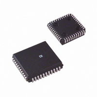
AD2S83IP-REEL Analog Devices Inc, AD2S83IP-REEL Datasheet - Page 16

AD2S83IP-REEL
Manufacturer Part Number
AD2S83IP-REEL
Description
IC R/D CONV TRACKING 44PLCC T/R
Manufacturer
Analog Devices Inc
Type
R/D Converterr
Datasheet
1.AD2S83IPZ-REEL.pdf
(19 pages)
Specifications of AD2S83IP-REEL
Rohs Status
RoHS non-compliant
Input Type
Parallel
Output Type
Digital
Interface
Parallel
Current - Supply
30mA
Mounting Type
Surface Mount
Package / Case
44-PLCC
SOURCES OF ERRORS
Integrator Offset
Additional inaccuracies in the conversion of the resolver signals
will result from an offset at the input to the integrator. This
offset will be treated as an error signal. The resulting angular
error will typically be 1 arc minute over the operating tempera-
ture range.
A description of how to adjust the zero offset is given in the
Component Selection section; the circuit required is shown in
Figure 1.
Differential Phase Shift
Phase shift between the sine and cosine signals from the resolver
is known as differential phase shift and can cause static error.
Some differential phase shift will be present on all resolvers as a
result of coupling. A small resolver residual voltage (quadrature
voltage) indicates a small differential phase shift. Additional
phase shift can be introduced if the sine channel wires and the
cosine channel wires are treated differently. For instance, differ-
ent cable lengths or different loads could cause differential phase
shift.
The additional error caused by differential phase shift on the
input signals approximates to
where a = differential phase shift (degrees).
This error can be minimized by choosing a resolver with a small
residual voltage, ensuring that the sine and cosine signals are
handled identically and removing the reference phase shift (see
the Connecting the Resolver section). By taking these precau-
tions the extra error can be made insignificant.
Most resolvers exhibit a phase shift between the signal and the
reference. This phase shift will, however, give rise under
dynamic conditions to an additional error defined by:
Under static operating conditions phase shift between the refer-
ence and the signal lines alone will not theoretically affect the
converter’s static accuracy.
For example, for a phase shift of 20 degrees, a shaft rotation of
22 rps and a reference frequency of 5 kHz, the converter will
exhibit an additional error of:
This effect can be eliminated by placing a phase shift in the
reference to the converter equivalent to the phase shift in the
resolver (see the Connecting the Resolver section).
Note: Capacitive and inductive crosstalk in the signal and reference
leads and wiring can cause similar problems.
AD2S83
Shaft Speed (rps) × Phase Shift (Degrees )
b = signal to reference phase shift (degrees).
Reference Frequency
Error = 0.53 a × b arc minutes
22 × 20
5000
= 0.088 Degrees
= Error Degrees
VELOCITY ERRORS
Some “ripple” or noise will always be present in the velocity
signal. Velocity signal ripple is caused by, or related to, the
following parameters. The resulting effects are generally addi-
tive. This means diagnosis needs to be an iterative process in
order to define the source of the error.
1.0 Reference Frequency
2.0 Resolver Inaccuracies
2.1 Sine and Cosine Amplitude Mismatch
2.2 Differential Phase Shift between the Sine and Cosine Inputs
3.0 LSB Update Ripple
3.1 Ripple due to the LSB rate given by:
4.0 Torque Ripple
A ripple content at the reference frequency is superimposed
on the velocity signal output. The amplitude depends on
the loop bandwidth. This error is a function of a dc offset at
the input to Phase Sensitive Demodulator (PSD).
Impedance mismatch occur in the sine and cosine windings
of the resolver. These give rise to differential phase shift
between the sine and cosine inputs to the RDC and varia-
tions in the resolver output amplitudes.
This is normally identified by the presence of asymmetrical
ripple voltages.
The frequency of this ripple is usually twice the input veloc-
ity, and the amplitude is proportional to the magnitude of
the velocity signal. The phase shift is normally induced
through the connections from the resolver to the converter.
Maintaining equal lengths of screened twisted pair cable
from the resolver to the AD2S83 will reduce the effects of
resistive imbalance, and therefore, reduce differential phase
shift.
LSB update noise occurs as the resolver rotates and the
digital outputs of the RDC are updated. For a correctly
scaled loop, this ripple component has a magnitude of
approximately 2 mV peak at 16-bit resolution.
The PSD generates sums and differences of all its compo-
nent input frequencies, so when the LSB update rate is an
multiple of the reference frequency, a beat frequency is
generated. The magnitude of this ripple is a function of the
LSB weighting, i.e., ripple is less at 16 bits.
Torque ripple is a phenomenon associated with motors. An
ac motor naturally exhibits a sinusoidal back emf. In an
ideal system the current fed to the motor should, in order
to cancel, also be sinusoidal. In practice the current is often
trapezoidal. Consequently, the output torque from the motor
will not be smooth and torque ripple is created. If the load-
ing on a motor is constant, the velocity of the motor shaft
will vary as a result of the cyclic variation of motor torque.
The variation in velocity then appears on the velocity
output as ripple. This is not an error but a true velocity
variation in the system.
LSB rate = N × Reference Frequency


