LM2512ASM/NOPB National Semiconductor, LM2512ASM/NOPB Datasheet - Page 5
LM2512ASM/NOPB
Manufacturer Part Number
LM2512ASM/NOPB
Description
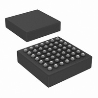
IC MPL1 SERIALIZER 24BIT 49UFBGA
Manufacturer
National Semiconductor
Series
LMr
Datasheet
1.LM2512ASMNOPB.pdf
(22 pages)
Specifications of LM2512ASM/NOPB
Function
Serializer
Data Rate
468Mbps
Input Type
LVCMOS
Output Type
LVCMOS
Number Of Inputs
21
Number Of Outputs
3
Voltage - Supply
1.6 V ~ 3 V
Operating Temperature
-30°C ~ 85°C
Mounting Type
Surface Mount
Package / Case
49-UFBGA
Lead Free Status / RoHS Status
Lead free / RoHS Compliant
Other names
LM2512ASMTR
Available stocks
Company
Part Number
Manufacturer
Quantity
Price
Company:

Part Number:
LM2512ASM/NOPB
Manufacturer:
National Semiconductor
Quantity:
1 955
Company:
Part Number:
LM2512ASM/NOPB
Manufacturer:
AD
Quantity:
4 858
Company:
Part Number:
LM2512ASM/NOPB
Manufacturer:
Texas Instruments
Quantity:
10 000


PIXEL CLOCK (PCLK)
f
PCLK
t
t
SPI INTERFACE
f
f
t
t
t
t
t
t
t
t
t
t
PCLK
T
STOPpclk
SCLw
SCLr
s0
s1
h1
w1h
w1l
r
f
0H
h0
w2
Symbol
Recommended Input Timing Requirements (PCLK and SPI)
Over recommended operating supply and temperature ranges unless otherwise specified. (Note 2)
Note 1: “Absolute Maximum Ratings” are those values beyond which the safety of the device cannot be guaranteed. They are not meant to imply that the device
should be operated at these limits. The tables of “Electrical Characteristics” specify conditions for device operation.
Note 2: Typical values are given for V
Note 3: Current into a device pin is defined as positive. Current out of device pins is defined as negative. Voltages are referenced to Ground unless otherwise
specified.
Note 4: For IDD tests - input signal conditions are: (swing, edge, freq, DE = H, VS = L, HS = L, RGB Checkerboard Pattern: AAAAAA-555555)
Note 5: Total Supply Current Conditions: checkerboard data pattern, 20MHz PCLK (3MDs), TYP V
= VDD = 2.0V.
Note 6: Enable Time is a complete MPL start up comprised of t0 + t1 + t2 + t3 + t4.
Note 7: Maximum transition time is a function of clock rate and should be less than 30% of the clock period to preserve signal quality.
Note 8: Guaranteed functionally by the I
Note 9: This is the minimum time that the PCLK needs to be held off for in order for the device to be reset. Once PCLK is reapplied, a PLL Lock is required and
start up sequence before video data is serialized.
Note 10: 1 UI is the serial data MD pulse width = 1 / 8xPCLK (3 MD lanes), 1 UI is the serial data MD pulse width = 1 / 12xPCLK (2 MD lanes)
Note 11: This is a functional parameter and is guaranteed by design or characterization.
DC
Pixel Clock Frequency
Pixel Clock Duty Cycle
Transition Time
Clock Stop Gap
SCL Frequency
CSX Set Time
SI Set Time
SI Hold Time
SCL Pulse Width High
SCL Pulse Width Low
SCL Rise Time
SCL Fall Time
SI Hold Time
CSX Hold Time
CSX OFF Time
Parameter
DDIO
DDZ
= 1.8V and V
parameter. See also Figure 10.
3 MD Lane, (4X)
2 MD Lane, (6X)
(Notes 7, 11)
(Notes 9, 11)
WRITE
READ
Figure 15
Figures 15, 16
Figure 15
DD
= V
DDA
= 1.8V and T
Conditions
WRITE
READ
WRITE
READ
5
A
= 25°C.
DDIO
= V
DDA
Min
100
7.5
30
60
30
30
35
60
35
60
30
65
5
2
4
= V
DD
= 1.8V, MAX VDDIO = 3.0V, MAX VDDA
Typ
>2
50
2
5
5
Max
22.5
6.67
15
70
10
www.national.com
cycles
PCLK
Units
MHz
MHz
MHz
MHz
ns
ns
ns
ns
ns
ns
ns
ns
ns
ns
ns
ns
ns
%
Related parts for LM2512ASM/NOPB
Image
Part Number
Description
Manufacturer
Datasheet
Request
R

Part Number:
Description:
Mobile Pixel Link Level 0, 24-bit Rgb Display Interface Serializer With Dithering And Look Up Table Option
Manufacturer:
National Semiconductor Corporation
Datasheet:

Part Number:
Description:
National Semiconductor [8-Bit D/A Converter]
Manufacturer:
National Semiconductor
Datasheet:
Part Number:
Description:
National Semiconductor [Media Coprocessor]
Manufacturer:
National Semiconductor
Datasheet:
Part Number:
Description:
Digitally Controlled Tone and Volume Circuit with Stereo Audio Power Amplifier, Microphone Preamp Stage and National 3D Sound
Manufacturer:
National Semiconductor
Datasheet:
Part Number:
Description:
Digitally Controlled Tone and Volume Circuit with Stereo Audio Power Amplifier, Microphone Preamp Stage and National 3D Sound
Manufacturer:
National Semiconductor
Datasheet:
Part Number:
Description:
AC97 Rev 2 Codec with Sample Rate Conversion and National 3D Sound
Manufacturer:
National Semiconductor
Part Number:
Description:
Manufacturer:
National Semiconductor
Datasheet:
Part Number:
Description:
Manufacturer:
National Semiconductor
Datasheet:
Part Number:
Description:
General Purpose, Low Voltage, Low Power, Rail-to-Rail Output Operational Amplifiers
Manufacturer:
National Semiconductor
Datasheet:
Part Number:
Description:
8-bit 20 MSPS flash A/D converter.
Manufacturer:
National Semiconductor
Datasheet:
Part Number:
Description:
Low Noise Quad Operational Amplifier
Manufacturer:
National Semiconductor
Datasheet:
Part Number:
Description:
Quad Differential Line Receivers
Manufacturer:
National Semiconductor
Datasheet:
Part Number:
Description:
Quad High Speed Trapezoidal? Bus Transceiver
Manufacturer:
National Semiconductor
Datasheet:
Part Number:
Description:
Dual Line Receiver
Manufacturer:
National Semiconductor
Datasheet: