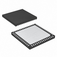
PI2EQX5864CZFE Pericom Semiconductor, PI2EQX5864CZFE Datasheet - Page 10

PI2EQX5864CZFE
Manufacturer Part Number
PI2EQX5864CZFE
Description
IC PCI-E REDRIVER 56TQFN
Manufacturer
Pericom Semiconductor
Series
ReDriver™r
Type
Redriverr
Datasheet
1.PI2EQX5864CZFE.pdf
(20 pages)
Specifications of PI2EQX5864CZFE
Tx/rx Type
CML
Capacitance - Input
50pF
Voltage - Supply
1.15 V ~ 1.25 V
Current - Supply
800mA
Mounting Type
Surface Mount
Package / Case
56-TQFN
Operating Temperature (min)
0C
Operating Temperature Classification
Commercial
Operating Temperature (max)
70C
Rad Hardened
No
Lead Free Status / RoHS Status
Lead free / RoHS Compliant
Delay Time
-
Lead Free Status / RoHS Status
Lead free / RoHS Compliant, Compliant
Available stocks
Company
Part Number
Manufacturer
Quantity
Price
Company:
Part Number:
PI2EQX5864CZFE
Manufacturer:
Pericom
Quantity:
135
Company:
Part Number:
PI2EQX5864CZFE
Manufacturer:
Pericom
Quantity:
367
Byte 2 - Loopback and Emphasis Control Register (LBEC)
LB_xyxy#=0=loopback mode, LB_xyxy#=1=normal mode, DE_x=0=pre-emphasis, DE_x=1=de-emphasis
Note: R=Read only, W=Write only, R/W=Read and Write, X=Undefi ned, rsvd=reserved for future use
Individual control for each lane is provided for the loopback function via this register.
BYTE 3 - Channel Input Disable (INDIS)
INDIS_xy=0=enable input, INDIS_xy=1=disable input
Note: R=Read only, W=Write only, R/W=Read and Write, X=Undefi ned, rsvd=reserved for future use
The Channel Input Disable register, provides control over the input buffer of each channel independently. When and INDIS_xy bit is
logic 1, then the input buffer is switched off and the input termination is high impedance. This feature can be used for PCB testing,
and when only one input is used during Loopback as a demux function. When INDIS_xy is at a logic 0 state then the input buffer is
enabled (normal operating mode).
BYTE 4 - Channel Output Disable (OUTDIS)
ODIS_xy=0=enable output, ODIS_xy=1=disable output
Note: R=Read only, W=Write only, R/W=Read and Write, X=Undefi ned, rsvd=reserved for future use
The Channel Output Disable register, allows control over the output buffer of each channel independently. When and OUTDIS_xy
bit is logic 1, then the output buffer is switched off and the termination is high impedance. This feature can be used for PCB testing,
and when only one output is used during Loopback as a mux function. When INDIS_xy is at a logic 0 state then the input buffer is
enabled (normal operating mode).
Power-on
Power-on
Power-on
Name
Name
Name
Type
State
Type
State
Type
State
Bit
Bit
Bit
09-0002
LB_A0B0#
INDIS_A0
ODIS_A0
R/W
R/W
R/W
LB#
7
7
0
7
0
LB_A1B1#
INDIS_B0
ODIS_B0
R/W
R/W
R/W
LB#
6
6
0
6
0
LB_A2B2#
INDIS_A1
ODIS_A1
R/W
R/W
R/W
LB#
5
5
0
5
0
LB_A3B3#
INDIS_B1
ODIS_B1
R/W
LB#
R/W
R/W
10
4
4
0
4
0
with Equalization, Emphasis and I
INDIS_A2
ODIS_A2
DE_A
R/W
R/W
R/W
3
1
3
0
3
0
5.0Gbps 4-Lane PCIe
INDIS_B2
ODIS_B2
DE_B
R/W
R/W
R/W
2
1
2
0
2
0
INDIS_A3
ODIS_A3
rsvd
R/W
R/W
®
X
R
1
1
0
1
0
2.0 ReDdriver™
PS8934D
PI2EQX5864C
2
INDIS_B3
C Control
ODIS_B3
rsvd
R/W
R/W
R
X
0
0
0
0
0
07/08/09


