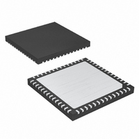
PI2EQX5864CZFE Pericom Semiconductor, PI2EQX5864CZFE Datasheet - Page 15

PI2EQX5864CZFE
Manufacturer Part Number
PI2EQX5864CZFE
Description
IC PCI-E REDRIVER 56TQFN
Manufacturer
Pericom Semiconductor
Series
ReDriver™r
Type
Redriverr
Datasheet
1.PI2EQX5864CZFE.pdf
(20 pages)
Specifications of PI2EQX5864CZFE
Tx/rx Type
CML
Capacitance - Input
50pF
Voltage - Supply
1.15 V ~ 1.25 V
Current - Supply
800mA
Mounting Type
Surface Mount
Package / Case
56-TQFN
Operating Temperature (min)
0C
Operating Temperature Classification
Commercial
Operating Temperature (max)
70C
Rad Hardened
No
Lead Free Status / RoHS Status
Lead free / RoHS Compliant
Delay Time
-
Lead Free Status / RoHS Status
Lead free / RoHS Compliant, Compliant
Available stocks
Company
Part Number
Manufacturer
Quantity
Price
Company:
Part Number:
PI2EQX5864CZFE
Manufacturer:
Pericom
Quantity:
135
Company:
Part Number:
PI2EQX5864CZFE
Manufacturer:
Pericom
Quantity:
367
Equalizer
Notes
1. K28.7 pattern is applied differentially at point A as shown in AC test circuit (see fi gure).
2. Total jitter does not include the signal source jitter. Total jitter (TJ) = (14.1 × RJ + DJ) where RJ is random RMS jitter and DJ is maximum deter-
ministic jitter. Signal source is a K28.5 ± pattern (00 1111 1010 11 0000 0101) for the deterministic jitter test and K28.7 (0011111000) or equivalent
for random jitter test. Residual jitter is that which remains after equalizing media-induced losses of the environment of Figure 1 or its equivalent.
The deterministic jitter at point B must be from media-induced loss, and not from clock source modulation. Jitter is measured at 0V at point C of
the AC test circuit (see fi gure).
CML Transmitter Output (VDD = 1.2V ± 0.05V, T
Notes:
1. Recommended external coupling capacitor.
Digital I/O DC Specifi cations (VDD = 1.2V ± 0.05V, T
Notes:
1. Includes input signals A1, A2, A4, LB#, MODE#, RESET#, RXD_[A:B], SCL, SDA
2. For control inputs without pullups: A1, A2, A4, SCL, SDA
3. Control inputs with pull-ups include: LB#, MODE#, RESET#, RXD_[A:B]
Symbol
J
J
J
Symbol
Z
Z
V
V
V
t
C
Symbol
V
V
V
V
V
I
I
I
F
IH
IL1
IL2
RS-T
RS-D
RM
OUT
TX-DIFF-DC
, t
TX
DIFFP
TX-DIFFP-P
TX-C
IH
IL
OH
OL
hys
(1)
R
(2)
(3)
(1)
09-0002
Parameters
DC input logic high
DC input logic low
DC output logic high
DC output logic low
Hysteresis of Schmitt
trigger input
Input high current
Input low current
Input low current
Parameters
Residual jitter
Residual jitter
Random jitter
Parameters
Output resistance
DC Differential TX Im-
pedance
Output Voltage Swing,
Differential
Differential Peak-to-peak
Ouput Voltage
Common-Mode Voltage
Transition Time
AC Coupling Capacitor
Conditions
I
I
OH
OL
Conditions
Total
Deterministic
Note 2
Conditions
Single ended
|VTX-D+ - VTX-D-|
VTX-DIFFP-P = 2 * | VTX-D+
- VTX-D- |
| VTX-D+ + VTX-D- | / 2
20% to 80% (3)
= 4mA
= 4mA
A
= 0 to 70°C)
A
= 0 to 70°C)
15
Min.
VDD/2 +0.2
-0.3
VDD-0.4
0.2
-20
-20
with Equalization, Emphasis and I
5.0Gbps 4-Lane PCIe
Typ.
Min.
200
Min.
40
80
0.4
75
Typ.
50
100
VDD- 0.3
Typ.
1.5
Max.
VDD+0.3
VDD/2 -0.2
0.4
100
®
Max.
0.3
0.2
2.0 ReDdriver™
Max.
60
120
1000
2.0
150
200
PS8934D
PI2EQX5864C
Units
V
V
V
V
V
uA
uA
uA
2
C Control
Units
Ohms
Ohms
mVp-p
V
V
ps
nF
Units
Ulp-p
Ulp-p
psrms
07/08/09


