PI2EQX5864CZFE Pericom Semiconductor, PI2EQX5864CZFE Datasheet - Page 9
PI2EQX5864CZFE
Manufacturer Part Number
PI2EQX5864CZFE
Description
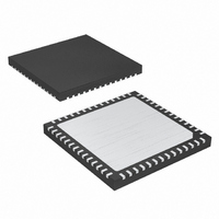
IC PCI-E REDRIVER 56TQFN
Manufacturer
Pericom Semiconductor
Series
ReDriver™r
Type
Redriverr
Datasheet
1.PI2EQX5864CZFE.pdf
(20 pages)
Specifications of PI2EQX5864CZFE
Tx/rx Type
CML
Capacitance - Input
50pF
Voltage - Supply
1.15 V ~ 1.25 V
Current - Supply
800mA
Mounting Type
Surface Mount
Package / Case
56-TQFN
Operating Temperature (min)
0C
Operating Temperature Classification
Commercial
Operating Temperature (max)
70C
Rad Hardened
No
Lead Free Status / RoHS Status
Lead free / RoHS Compliant
Delay Time
-
Lead Free Status / RoHS Status
Lead free / RoHS Compliant, Compliant
Available stocks
Company
Part Number
Manufacturer
Quantity
Price
Company:

Part Number:
PI2EQX5864CZFE
Manufacturer:
Pericom
Quantity:
135
Company:
Part Number:
PI2EQX5864CZFE
Manufacturer:
Pericom
Quantity:
367


Acknowledge
Data transfer with acknowledge is required from the master. When the master releases the SDA line (HIGH) during the acknowledge
clock pulse, the PI2EQX5864C will pull down the SDA line during the acknowledge clock pulse so that it remains stable LOW dur-
ing the HIGH period of this clock pulse as indicated in the I
edge after each byte has been received.
Data Transfer
A data transfer cycle begins with the master issuing a start bit. After recognizing a start bit, the PI2EQX5864C will watch the next
byte of information for a match with its address setting. When a match is found it will respond with a read or write of data on the
following clocks. Each byte must be followed by an acknowledge bit, except for the last byte of a read cycle which ends with a stop
bit. For a write cycle, the fi rst data byte following the address byte is a dummy or fi ll byte that is not used by the PI2EQX5864C.
This byte is provided to provided compatibility with systems implementing 10-bit addressing. Data is transferred with the most
signifi cant bit (MSB) fi rst. After each block write, address pointer will reset to byte 0.
Register Description
Byte 0 - Signal Detect (SIG)
SIG_xy=0=low input signal, SIG_xy=1=valid input signal
Note: R=Read only, W=Write only, R/W=Read and Write, X=Undefi ned, rsvd=reserved for future use
The Signal Detect register provides information on the instantaneous status of the channel input from the Input Level Threshold
Detect circuit. If the input level falls below the Vth- level the relevant SIG_xy bit will be 0, indicating a low-level noise or electri-
cal idle input, resulting in the outputs going to the high-impedance off state or squelch mode. If the input level is above Vth-, then
SIG_xy is 1, indicating a valid input signal, and active signal recovery operation.
Byte 1 - Receiver Detect Output Register (RX50)
RX50_xy = 1 = load detected, RX50_xy = 0 = No receiver found
Note: R=Read only, W=Write only, R/W=Read and Write, X=Undefi ned, rsvd=reserved for future use
The RX50_xy bits report the result of a receiver detection cycle. One bit is assigned for each channel of the device. RX50_xy is
at a logic 1 level indicating a load and receiver was detected. When RX50_xy is 0 then a load device was not detected. The RX50
register is read-only, and is undefi ned after power-up until a Receiver Detection cycle completes.
Power-on
Power-on
Name
Name
Type
State
Type
State
Bit
Bit
09-0002
RX50_A0
SIG_A0
X
R
7
R
X
7
RX50_B0
SIG_B0
X
R
6
X
R
6
RX50_A1
SIG_A1
R
X
5
X
R
5
2
C Data Transfer diagram. The PI2EQX5864C will generate an acknowl-
RX50_B1
SIG_B1
R
X
4
R
X
4
9
with Equalization, Emphasis and I
RX50_A2
SIG_A2
R
X
R
X
3
3
5.0Gbps 4-Lane PCIe
RX50_B2
SIG_B2
R
X
X
2
R
2
RX50_A3
SIG_A3
®
X
X
R
R
1
1
2.0 ReDdriver™
PS8934D
PI2EQX5864C
2
C Control
RX50_B3
SIG_B3
X
R
X
R
0
0
07/08/09
Related parts for PI2EQX5864CZFE
Image
Part Number
Description
Manufacturer
Datasheet
Request
R

Part Number:
Description:
Fast CMOS bus interface register
Manufacturer:
Pericom Semiconductor
Datasheet:
Part Number:
Description:
4-bit,4-port bus exchange switch
Manufacturer:
Pericom Semiconductor
Datasheet:
Part Number:
Description:
Manufacturer:
Pericom Semiconductor
Datasheet:
Part Number:
Description:
Manufacturer:
Pericom Semiconductor
Datasheet:
Part Number:
Description:
Manufacturer:
Pericom Semiconductor
Datasheet:
Part Number:
Description:
Manufacturer:
Pericom Semiconductor
Datasheet:
Part Number:
Description:
Manufacturer:
Pericom Semiconductor
Datasheet:
Part Number:
Description:
Manufacturer:
Pericom Semiconductor
Datasheet:
Part Number:
Description:
Manufacturer:
Pericom Semiconductor
Datasheet:
Part Number:
Description:
Manufacturer:
Pericom Semiconductor
Datasheet:
Part Number:
Description:
Manufacturer:
Pericom Semiconductor
Datasheet:
Part Number:
Description:
Manufacturer:
Pericom Semiconductor
Datasheet:
Part Number:
Description:
Manufacturer:
Pericom Semiconductor
Datasheet:
Part Number:
Description:
Manufacturer:
Pericom Semiconductor
Datasheet: