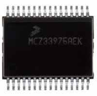
MCZ33975AEK Freescale Semiconductor, MCZ33975AEK Datasheet - Page 12

MCZ33975AEK
Manufacturer Part Number
MCZ33975AEK
Description
IC MULTIPLE SWITCH DETECT 32SOIC
Manufacturer
Freescale Semiconductor
Datasheet
1.MCZ33975AEK.pdf
(34 pages)
Specifications of MCZ33975AEK
Applications
Automotive
Interface
SPI
Voltage - Supply
5.5 V ~ 28 V
Package / Case
32-SOIC (7.5mm Width) Exposed Pad, 32-eSOIC, 32-HSOIC
Mounting Type
Surface Mount
Lead Free Status / RoHS Status
Lead free / RoHS Compliant
provide systems with ultra-low quiescent sleep/wake-up
modes and a robust interface between switch contacts and a
microprocessor. The 33975 replaces many of the discrete
components required when interfacing to microprocessor-
based systems while providing switch ground offset
protection, contact wetting current, and system wake-up.
switch-to-battery inputs and 14 switch-to-ground inputs. All
CHIP SELECT (CS)
communication using the chip select (
logic low state, command words may be sent to the 33975 via
the serial input (SI) pin, and switch status information can be
received by the MCU via the serial output (SO) pin. The
falling edge of
the
and low-to-high transitions of the
SCLK is in a logic low state. A clean CS signal is needed to
ensure no incomplete SPI words are sent to the device.
Internal to the 33975 device is an active pull-up to VDD on
CS
wake up the 33975 device. Data received from the device
during
SERIAL CLOCK (SCLK)
register of the 33975. The SI data is latched into the input
shift register on the falling edge of SCLK signal. The SO pin
shifts the switch status bits out on the rising edge of SCLK.
The SO data is available for the MCU to read on the falling
edge of SCLK. False clocking of the shift register must be
avoided to ensure validity of data. It is essential the SCLK pin
be in a logic low state whenever
this reason, it is recommended, though not necessary, that
the SCLK pin is commanded to a low logic state as long as
the device is not accessed and
When the
and SI pin will be ignored and the SO pin is tri-state.
12
33975
FUNCTIONAL DESCRIPTIONS
INTRODUCTION
1. Disables the SO driver (high-impedance)
1.
1. Activates the received command word, allowing the
The 33975 device is an integrated circuit designed to
The 33975 features 8-programmable switch-to-ground or
The system MCU selects the 33975 to receive
Rising edge of the
To avoid any spurious data, it is essential the high-to-low
In Sleep Mode the negative edge of
The system clock (SCLK) pin clocks the internal shift
.
INT
INT
switch changes occur during
page 11).
33975 to act upon new data from switch inputs.
CS
pin, and the state of the external switch inputs.
pin is reset to logic [1], except when additional
CS
wake-up may not be accurate.
is in a logic high state, any signal on the SCLK
CS
enables the SO output, latches the state of
CS
initiates the following operation:
CS
CS
CS
CS
makes any transition. For
is in a logic high state.
signal occur only when
CS
low (see
CS
) pin. With
FUNCTIONAL DESCRIPTIONS
(VDD applied) will
FUNCTIONAL PIN DESCRIPTION
Figure
CS
INTRODUCTION
6,
in a
switch inputs may be read as analog inputs through the
analog multiplexer (AMUX). Other features include a
programmable wake-up timer, programmable interrupt timer,
programmable wake-up/interrupt bits, and programmable
wetting current settings.
applications but may be used in a variety of other applications
such as computer, telecommunications, and industrial
controls.
SERIAL INPUT (SI)
information is latched into the input register on the falling
edge of SCLK. A logic high state present on SI will program
a one in the command word on the rising edge of the
signal. To program a complete word, 24 bits of information
must be entered into the device.
SERIAL OUTPUT (SO)
remains tri-stated until the
state. All open switches are reported as a zero, all closed
switches are reported as a one. The negative transition of
enables the SO driver.
data bit 24 available on the SO pin. Each successive positive
clock will make the next status data bit available for the MCU
to read on the falling edge of SCLK. The SI/SO shifting of the
data follows a first-in-first-out protocol, with both input and
output words transferring the most significant bit (MSB) first.
INTERRUPT OUTPUT (INT)
The
VDD. In Normal Mode, a switch state change will trigger the
INT
edge of
will not clear with rising edge of
has occurred while the
VDD on (Sleep Mode), the falling edge of
33975s in Normal Mode.
WAKE INPUT (WAKE)
input. The pin is designed to control a power supply Enable
pin. In the Normal Mode, the
Mode, the
the internal +5.0V supply.
This device is designed primarily for automotive
The SI pin is used for serial instruction data input. SI
The SO pin is the output from the shift register. The SO pin
The first positive transition of SCLK will make the status
The
In a multiple 33975 device system with
The
pin (when enabled). The
INT
INT
WAKE
CS
pin is an open-drain output with an internal pull-up to
WAKE
, and cleared on the rising edge of
pin is an interrupt output from the 33975 device.
pin is an open-drain output and a wake-up
pin is high. The
Analog Integrated Circuit Device Data
CS
CS
was low.
INT
WAKE
pin transitions to a logic low
CS
pin is latched on the falling
WAKE
if a switch contact change
Freescale Semiconductor
pin is low. In the Sleep
pin has a pull-up to
INT
WAKE
CS
will place all
. The
high and
INT
CS
pin
CS


