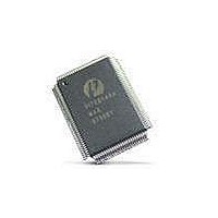
PI7C7300DNAE Pericom Semiconductor, PI7C7300DNAE Datasheet - Page 17

PI7C7300DNAE
Manufacturer Part Number
PI7C7300DNAE
Description
IC PCI-PCI BRIDGE 3PORT 272-BGA
Manufacturer
Pericom Semiconductor
Datasheet
1.PI7C7300DNAE.pdf
(107 pages)
Specifications of PI7C7300DNAE
Applications
*
Interface
*
Voltage - Supply
*
Package / Case
272-PBGA
Mounting Type
Surface Mount
Maximum Operating Temperature
+ 85 C
Minimum Operating Temperature
- 40 C
Mounting Style
SMD/SMT
Operating Supply Voltage
3 V to 3.6 V
Supply Current (max)
660 mA
Lead Free Status / RoHS Status
Lead free / RoHS Compliant
Available stocks
Company
Part Number
Manufacturer
Quantity
Price
Company:
Part Number:
PI7C7300DNAE
Manufacturer:
Pericom
Quantity:
135
Company:
Part Number:
PI7C7300DNAE
Manufacturer:
MAX
Quantity:
5 510
3.4
3.5
3.6
Pericom Semiconductor
CLOCK SIGNALS
MISCELLANEOUS SIGNALS
COMPACT PCI HOT-SWAP SIGNALS
Name
S_CFN#
Name
P_CLK
S1_CLKOUT
[7:0]
S2_CLKOUT
[7:0]
Name
BY_PASS
PLL_TM
S_CLKIN
SCAN_TM#
SCAN_EN
Name
LOO
HS_SW#
Pin #
Y2
Pin #
V6
A11, C12, A13,
B14, B15, C16,
A18, A19
T3, T1, P3, N3,
M4, L3, L2, J1
Pin #
Y4
Y3
V5
V4
U5
Pin #
U1
T2
Page 17 of 107
Type
PIU
Type
PI
PTS
PTS
Type
PI
PI
PI
PI
PID
Type
PO
PI
Description
Secondary Bus Central Function Control Pin. When
tied LOW, it enables the internal arbiter. When tied
HIGH, an external arbiter must be used. S1_REQ#[0]
or S2_REQ#[0] is reconfigured to be the secondary bus
grant input, and S1_GNT#[0] or S2_GNT#[0] is
reconfigured to be the secondary bus request output.
Description
Primary Clock Input. Provides timing for all
transactions on the primary interface.
Secondary Clock Output. Provides secondary 1
clocks phase synchronous with the P_CLK.
Secondary Clock Output. Provides secondary 2
clocks phase synchronous with the P_CLK.
Description
Reserved. Reserved for future use. Must be tied
HIGH.
Reserved. Reserved for future use. Must be tied
LOW.
Reserved. Reserved for future use. Must be tied
LOW.
Full-Scan Test Mode Enable (Active LOW).
Connect HIGH for normal operation.
When SCAN_TM# is active, the ten scan chains will be
enabled. The scan clock is P_CLK. The scan input and
outputs are as follows:
S1_REQ[6], S1_REQ[5], S1_REQ[4], S1_REQ[3],
S1_REQ[2], S2_REQ#[6], S2_REQ#[5], S2_REQ#[4],
S2_REQ#[3], S2_REQ#[2], and S1_GNT#[6],
S1_GNT#[5], S1_GNT#[4], S1_GNT#[3],
S1_GNT#[2], S2_GNT#[6], S2_GNT#[5],
S2_GNT#[4], S2_GNT#[3], S2_GNT#[2]
Full-Scan Enable Control. SCAN_EN should be tied
LOW in normal mode. When SCAN_EN is LOW, full-
scan is in shift operation if SCAN_TM# is active.
When SCAN_EN is HIGH, full-scan is in parallel
operation if SCAN_TM# is active.
Description
Hot Swap LED. The output of this pin lights a blue
LED to indicate insertion and removal ready status. If
HS_EN is LOW, pin is S2_GNT#[7].
Hot Swap Switch. When driven LOW, this signal
indicates that the board ejector handle indicates an
insertion or impending extraction of a board. If HS_EN
is LOW, pin is S2_REQ#[7].
3-PORT PCI-TO-PCI BRIDGE
November 2005 - Revision 1.01
PI7C7300D


