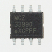
MCZ33990EF Freescale Semiconductor, MCZ33990EF Datasheet - Page 12

MCZ33990EF
Manufacturer Part Number
MCZ33990EF
Description
IC TRANSCEIVER J-1850 BUS 8-SOIC
Manufacturer
Freescale Semiconductor
Datasheet
1.MC33990D.pdf
(16 pages)
Specifications of MCZ33990EF
Applications
*
Interface
*
Voltage - Supply
*
Package / Case
8-SOIC (3.9mm Width)
Mounting Type
Surface Mount
Lead Free Status / RoHS Status
Lead free / RoHS Compliant
Available stocks
Company
Part Number
Manufacturer
Quantity
Price
Company:
Part Number:
MCZ33990EF
Manufacturer:
Freescale
Quantity:
4 702
Part Number:
MCZ33990EFR2
Manufacturer:
ON/安森美
Quantity:
20 000
Transmitter Data from the MCU (TX)
buffer with hysteresis for noise immunity purposes. This pin is a
5.0 V CMOS logic level input from the MCU following a true
logic protocol. A logic [0] input drives the BUS output to 0 V (via
the external pull-down resistor to ground on each node), while
a logic [1] input produces a high voltage at the BUS output. A
logic [0] input level is guaranteed when the Tx input pin is an
open-circuit by virtue of an internal 40 kΩ pull-down resistor. No
external resistor is required for its operation.
Transceiver Output (BUS)
Its output follows the waveshaped waveform input. Its output
voltage is limited to 6.25 V to 8.0 V under normal battery level
conditions. The limited level is controlled by an internal
regulator/clamp circuit. Once the battery voltage drops below
9.0 V, the regulator / clamp circuit saturates, causing the bus
voltage to track the battery voltage. A 1.5 kΩ ± 5% external
resistor (as well as any 10.6 kΩ pull-down resistors of any
secondary nodes) sinks the current to discharge the capacitors
during high-to-low transitions. This sourcing output is short
circuit-protected (60 mA to 170 mA) against a short to -2.0 V
and sinks less than 1.0 mA when shorted to V
occurs, the overtemperature shutdown circuit protects the
source driver of the device. In the event battery power is lost to
the assembly, the bus transmitter's output stage will be disabled
and the leakage current from the BUS output will not source or
sink more than 100 mA of current. The transceiver will operate
with a remote ground offset of ± 2.0 V, but the lower corners of
transmission will not be rounded during this condition.
Receiver Output to the Microcontroller (RX)
send received data to the microcontroller. It does not require an
external pull-up resistor to be used. The receiver is always
enabled and draws less than 65 µA of current from V
receive threshold is dependent on the state of the
The initial state of this output is always a logic [0] after supply
voltage is applied, but before the
state. The receiver circuitry is able to operate with V
voltages as low as 4.25 V and still remains capable of “waking
up” the 33990 when remote Class B activity is detected.
the bus, the receiver passes the bus message through to the
microcontroller. The 33990 does not automatically “wake up”
12
33990
TYPICAL APPLICATIONS
FUNCTIONAL PIN DESCRIPTION
The Tx input is a push-pull (N-channel / P-channel FETs)
This is the output driver stage that sources current to the bus.
This is a 5.0 V CMOS compatible push-pull output used to
When the
SLEEP
pin is low and message activity occurs on
SLEEP
pin goes to a logic [1]
BAT
TYPICAL APPLICATIONS
CLASS B MODULE OUTPUTS
. If a short
CLASS B MODULE INPUTS
SLEEP
BAT
BAT
. The
pin.
Waveshaping and 4X / Loop
5.0 V = waveshaping is disabled for 4X transmitting, and high
impedance = loopback mode of operation. This is a logic level
input used to select whether waveshaping for the Class B
output is enabled or disabled. A logic [0] enables waveshaping,
while a logic [1] disables waveshaping. In the 4X mode, the
BUS output rise time is less than 2.0 μs and the fall time is less
than 5.0 μs (owing to the external RC pull-down to ground). In
the loopback condition, the Tx signal is fed back to the Rx
output after waveshaping without being transmitted onto the
BUS. This mode of operation is useful for system diagnostic
purposes.
from a sleep state when bus activity occurs: the microcontroller
must tell it to do so.
voltage for Rx is specified as 4.75 V over an operating range of
-40°C to 125°C temperature and 7.0 V to 16 V V
maximum Rx voltage is compatible with the minimum V
voltage of microcontrollers to prevent the 33990 from sourcing
current to the microcontroller's output.
Switched Ground Output (LOAD)
pulls down the external resistor between the BUS and LOAD
outputs. In the event ground is lost to the assembly, the LOAD
output will bias itself “off” and will not leak more than 100 μA of
current out of this pin.
Overtemperature Shutdown
duration, an overtemperature shutdown circuit “latches off” the
output source transistor whenever the die temperature exceeds
150°C to 190°C. The output transistor remains latched off until
the Tx input is toggled from a logic [0] to a logic [1]. The rising
edge provides the clearing function, provided the locally sensed
temperature is 10°C to 15°C below the latch-off temperature trip
temperature.
Waveshaping
radiated EMI emissions.
Receiver Protocol
width (VPW) protocol. The microcontroller provides the VPW
decoding function. Once the receiver detects a transition on Rx,
it starts an internal counter. The initial “start of frame” bit is a
logic [1] and lasts 200 μs. For subsequent bits, if there is a bus
This input is a tristateable input: 0 V = normal waveshaping,
In the Static Electrical Characteristics table, the maximum
Normally this output is a saturated switch to ground, which
If the BUS output becomes shorted to ground for any
Waveshaping is incorporated into the 33990 to minimize
The Class B communication scheme uses a variable pulse
Analog Integrated Circuit Device Data
Freescale Semiconductor
BAT
. This
DD


