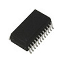
IDT6116SA45SOG IDT, Integrated Device Technology Inc, IDT6116SA45SOG Datasheet - Page 2

IDT6116SA45SOG
Manufacturer Part Number
IDT6116SA45SOG
Description
Manufacturer
IDT, Integrated Device Technology Inc
Datasheet
1.IDT6116SA45SOG.pdf
(11 pages)
Specifications of IDT6116SA45SOG
Density
16Kb
Access Time (max)
45ns
Sync/async
Asynchronous
Architecture
Not Required
Clock Freq (max)
Not RequiredMHz
Operating Supply Voltage (typ)
5V
Address Bus
11b
Package Type
SOIC
Operating Temp Range
0C to 70C
Number Of Ports
1
Supply Current
100mA
Operating Supply Voltage (min)
4.5V
Operating Supply Voltage (max)
5.5V
Operating Temperature Classification
Commercial
Mounting
Surface Mount
Pin Count
24
Word Size
8b
Number Of Words
2K
Lead Free Status / Rohs Status
Compliant
Pin Configurations
Pin Description
Truth Table
NOTE:
1. H = V
Standby
Read
Read
Write
IDT6116SA/LA
CMOS Static RAM 2K (16K x 8-Bit)
IH
Mode
, L = V
I/O
GND
A
I/O
I/O
I/O
Name
0
GND
0
WE
V
CS
OE
A
A
A
A
A
A
A
A
- A
CC
- I/O
IL
6
5
4
7
3
2
1
0
0
1
2
, X = Don't Care.
10
7
DIP/SOIC/SOJ
(1)
10
1
2
3
4
5
6
7
8
9
11
12
Top View
CS
H
L
L
L
SO24-2
SO24-4
D24-2
D24-1
P24-2
P24-1
OE
X
H
X
L
Data Input/Output
Address Inputs
Output Enable
Write Enable
24
23
22
21
20
19
18
17
16
15
14
13
Description
Chip Select
Ground
Power
3089 drw 02
WE
X
H
H
L
V
A
A
A
WE
OE
CS
I/O
I/O
I/O
I/O
I/O
CC
10
8
9
7
6
5
4
3
DATA
DATA
High-Z
High-Z
,
I/O
3089 tbl 02
3089 tbl 01
OUT
IN
2
Capacitance
NOTE:
1. This parameter is determined by device characterization, but is not production
NOTES:
1. Stresses greater than those listed under ABSOLUTE MAXIMUM RATINGS
2. V
Absolute Maximum Ratings
C
C
P
I
V
T
T
T
OUT
A
BIAS
STG
IN
I/O
T
TERM
Symbol
Symbol
tested.
may cause permanent damage to the device. This is a stress rating only and
functional operation of the device at these or any other conditions above those
indicated in the operational sections of this specification is not implied. Exposure
to absolute maximum rating conditions for extended periods may affect
reliability.
TERM
(2)
Military, Commercial, and Industrial Temperature Ranges
must not exceed V
Input Capacitance
I/O Capacitance
Operating
Under Bias
Storage Temperature
Power Dissipation
DC Output Current
Terminal Voltage
with Respect
to GND
Temperature
Temperature
Parameter
Rating
CC
(T
(1)
+0.5V.
A
= +25°C, f = 1.0 MH
-0.5 to +7.0
-55 to +125
-55 to +125
0 to +70
Com'l.
Conditions
1.0
50
V
V
OUT
IN
= 0V
= 0V
-0.5 to +7.0
-55 to +125
-65 to +135
-65 to +150
Mil.
1.0
(1)
50
Max.
8
8
Z
)
3089 tbl 04
3089 tbl 03
Unit
Unit
pF
pF
mA
o
o
o
W
V
C
C
C


