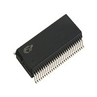
CY7C68001-56PVC Cypress Semiconductor Corp, CY7C68001-56PVC Datasheet - Page 13

CY7C68001-56PVC
Manufacturer Part Number
CY7C68001-56PVC
Description
Manufacturer
Cypress Semiconductor Corp
Datasheet
1.CY7C68001-56PVC.pdf
(45 pages)
Specifications of CY7C68001-56PVC
Operating Temperature (min)
0C
Operating Temperature Classification
Commercial
Operating Temperature (max)
70C
Package Type
SSOP
Rad Hardened
No
Lead Free Status / Rohs Status
Not Compliant
8.1 CY7C68001 Pin Definitions
Table 8-1. SX2 Pin Definitions
Document #: 38-08013 Rev. *K
QFN
Pin
42
54
33
34
35
36
37
38
39
40
18
19
20
21
22
23
24
25
45
46
47
48
49
50
51
3
6
9
8
5
4
SSOP
Pin
10
13
16
15
49
12
40
41
42
43
44
45
46
47
25
26
27
28
29
30
31
32
52
53
54
55
56
11
5
1
2
FIFOADR2
FIFOADR0
FIFOADR1
XTALOUT
FLAGD/C
DMINUS
PKTEND
RESET#
XTALIN
READY
DPLUS
FD[10]
FD[12]
FD[13]
FD[14]
AGND
FD[11]
Name
AVCC
SLOE
FD[0]
FD[1]
FD[2]
FD[3]
FD[4]
FD[5]
FD[6]
FD[7]
FD[8]
FD[9]
INT#
NC
S#
FLAGD:O
Output
Output
Output
Output
Power
Power
CS#:I
Type
I/O/Z
I/O/Z
Input
Input
Input
Input
Input
Input
Input
I/O/Z
I/O/Z
I/O/Z
I/O/Z
I/O/Z
I/O/Z
I/O/Z
I/O/Z
I/O/Z
I/O/Z
I/O/Z
I/O/Z
I/O/Z
I/O/Z
I/O/Z
Default
N/A
N/A
N/A
N/A
N/A
O
H
Z
Z
L
I
I
I
I
I
I
I
I
I
I
I
I
I
I
I
I
I
I
I
I
I
Analog V
Analog Ground. Connect to ground with as short a path as possible.
USB D– Signal. Connect to the USB D– signal.
USB D+ Signal. Connect to the USB D+ signal.
Active LOW Reset. Resets the entire chip. This pin is normally tied to V
through a 100K resistor, and to GND through a 0.1-μF capacitor.
Crystal Input. Connect this signal to a 24 MHz parallel-resonant, fundamental
mode crystal and 20 pF capacitor to GND. It is also correct to drive XTALIN with
an external 24 MHz square wave derived from another clock source.
Crystal Output. Connect this signal to a 24 MHz parallel-resonant, fundamental
mode crystal and 20 pF capacitor to GND. If an external clock is used to drive
XTALIN, leave this pin open.
No Connect. This pin must be left unconnected.
READY is an output-only ready that gates external command reads and writes.
Active High.
INT# is an output-only external interrupt signal. Active Low.
SLOE is an input-only output enable with programmable polarity (POLAR.4) for
the slave FIFOs connected to FD[7:0] or FD[15:0].
FIFOADR2 is an input-only address select for the slave FIFOs connected to
FD[7:0] or FD[15:0].
FIFOADR0 is an input-only address select for the slave FIFOs connected to
FD[7:0] or FD[15:0].
FIFOADR1 is an input-only address select for the slave FIFOs connected to
FD[7:0] or FD[15:0].
PKTEND is an input-only packet end with programmable polarity (POLAR.5) for
the slave FIFOs connected to FD[7:0] or FD[15:0].
FLAGD is a programmable slave-FIFO output status flag signal. CS# is a master
chip select (default).
FD[0] is the bidirectional FIFO/Command data bus.
FD[1] is the bidirectional FIFO/Command data bus.
FD[2] is the bidirectional FIFO/Command data bus.
FD[3] is the bidirectional FIFO/Command data bus.
FD[4] is the bidirectional FIFO/Command data bus.
FD[5] is the bidirectional FIFO/Command data bus.
FD[6] is the bidirectional FIFO/Command data bus.
FD[7] is the bidirectional FIFO/Command data bus.
FD[8] is the bidirectional FIFO data bus.
FD[9] is the bidirectional FIFO data bus.
FD[10] is the bidirectional FIFO data bus.
FD[11] is the bidirectional FIFO data bus.
FD[12] is the bidirectional FIFO data bus.
FD[13] is the bidirectional FIFO data bus.
FD[14] is the bidirectional FIFO data bus.
CC
. This signal provides power to the analog section of the chip.
Description
CY7C68001
Page 13 of 45
CC
[+] Feedback
[+] Feedback
[+] Feedback


