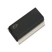
CY7C68001-56PVC Cypress Semiconductor Corp, CY7C68001-56PVC Datasheet - Page 14

CY7C68001-56PVC
Manufacturer Part Number
CY7C68001-56PVC
Description
Manufacturer
Cypress Semiconductor Corp
Datasheet
1.CY7C68001-56PVC.pdf
(45 pages)
Specifications of CY7C68001-56PVC
Operating Temperature (min)
0C
Operating Temperature Classification
Commercial
Operating Temperature (max)
70C
Package Type
SSOP
Rad Hardened
No
Lead Free Status / Rohs Status
Not Compliant
Table 8-1. SX2 Pin Definitions (continued)
Document #: 38-08013 Rev. *K
QFN
Pin
52
29
30
31
13
14
44
15
16
55
11
17
27
32
43
53
56
10
12
26
28
41
1
2
7
SSOP
Pin
36
37
38
20
21
51
22
23
14
18
24
34
39
50
17
19
33
35
48
3
8
9
6
4
7
Reserved
WAKEUP
FLAGA
FLAGB
FLAGC
FD[15]
SLWR
IFCLK
Name
SLRD
GND
GND
GND
GND
GND
GND
GND
SCL
SDA
V
V
V
V
V
V
V
CC
CC
CC
CC
CC
CC
CC
Ground
Ground
Ground
Ground
Ground
Ground
Ground
Output
Output
Output
Power
Power
Power
Power
Power
Power
Power
Type
I/O/Z
Input
Input
I/O/Z
Input
Input
OD
OD
Default
N/A
N/A
N/A
N/A
N/A
N/A
N/A
N/A
N/A
N/A
N/A
N/A
N/A
N/A
N/A
N/A
N/A
N/A
H
H
H
Z
Z
Z
I
FD[15] is the bidirectional FIFO data bus.
SLRD is the input-only read strobe with programmable polarity (POLAR.3) for the
slave FIFOs connected to FD[7:0] or FD[15:0].
SLWR is the input-only write strobe with programmable polarity (POLAR.2) for
the slave FIFOs connected to FD[7:0] or FD[15:0].
FLAGA is a programmable slave-FIFO output status flag signal.
Defaults to PF for the FIFO selected by the FIFOADR[2:0] pins.
FLAGB is a programmable slave-FIFO output status flag signal.
Defaults to FULL for the FIFO selected by the FIFOADR[2:0] pins.
FLAGC is a programmable slave-FIFO output status flag signal.
Defaults to EMPTY for the FIFO selected by the FIFOADR[2:0] pins.
Interface Clock, used for synchronously clocking data into or out of the slave
FIFOs. IFCLK also serves as a timing reference for all slave FIFO control signals.
When using the internal clock reference (IFCONFIG.7=1) the IFCLK pin can be
configured to output 30/48 MHz by setting bits IFCONFIG.5 and IFCONFIG.6.
IFCLK may be inverted by setting the bit IFCONFIG.4=1. Programmable polarity.
Reserved. Must be connected to ground.
USB Wakeup. If the SX2 is in suspend, asserting this pin starts up the oscillator
and interrupts the SX2 to allow it to exit the suspend mode. During normal
operation, holding WAKEUP asserted inhibits the SX2 chip from suspending. This
pin has programmable polarity (POLAR.7).
I
EEPROM is attached.
I
is attached.
V
V
V
V
V
V
V
Connect to ground.
Connect to ground.
Connect to ground.
Connect to ground.
Connect to ground.
Connect to ground.
Connect to ground.
2
2
CC
CC
CC
CC
CC
CC
CC
C Clock. Connect to V
C Data. Connect to V
. Connect to 3.3V power source.
. Connect to 3.3V power source.
. Connect to 3.3V power source.
. Connect to 3.3V power source.
. Connect to 3.3V power source.
. Connect to 3.3V power source.
. Connect to 3.3V power source.
CC
CC
with a 2.2K-10 KOhms resistor, even if no I
with a 2.2K-10 KOhms resistor, even if no I
Description
CY7C68001
2
C EEPROM
2
Page 14 of 45
C
[+] Feedback
[+] Feedback
[+] Feedback


