LMX2326TM National Semiconductor, LMX2326TM Datasheet - Page 2
LMX2326TM
Manufacturer Part Number
LMX2326TM
Description
Manufacturer
National Semiconductor
Type
PLL Frequency Synthesizerr
Datasheet
1.LMX2326TM.pdf
(19 pages)
Specifications of LMX2326TM
Number Of Elements
1
Supply Current
7mA
Pll Input Freq (min)
100MHz
Pll Input Freq (max)
2.8GHz
Operating Supply Voltage (typ)
3V
Operating Temp Range
-40C to 85C
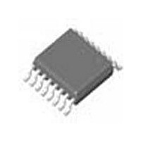
Package Type
TSSOP
Operating Supply Voltage (min)
2.3V
Operating Supply Voltage (max)
5.5V
Operating Temperature Classification
Industrial
Pin Count
16
Lead Free Status / Rohs Status
Not Compliant
Available stocks
Company
Part Number
Manufacturer
Quantity
Price

Part Number:
LMX2326TMD
Manufacturer:
NS/国半
Quantity:
20 000
Company:
Part Number:
LMX2326TMX
Manufacturer:
NS
Quantity:
1 228
Part Number:
LMX2326TMX
Manufacturer:
NS/国半
Quantity:
20 000


www.national.com
TSSOP
16-Pin
Connection Diagrams
Pin Descriptions
10
11
12
13
14
15
16
1
2
3
4
5
6
7
8
9
Order Number LMX2306TM, LMX2306TMX, LMX2316TM,
16-Lead (0.173” Wide) Thin Shrink Small Outline
16-Pin
CSP
15
16
10
11
12
13
14
1
2
3
4
5
6
7
8
9
See NS Package Number MTC16
OSC
LMX2326TM or LMX2326TMX
Name
Fo/LD
Clock
V
V
GND
GND
GND
Data
CP
Pin
FL
CE
LE
V
f
f
CC1
CC2
IN
IN
P
o
o
IN
LMX2306/16/26
LMX2316TMX,
Package(TM)
I/O
O FastLock Output. For connection of parallel resistor to the loop filter. (See Section 1.3.4 FASTLOCK
O Charge Pump Output. For connection to a loop filter for driving the input of an external VCO.
O Multiplexed Output of the RF Programmable or Reference Dividers and Lock Detect. CMOS output.
I
I
I
I
I
I
I
MODES description.)
Charge Pump Ground.
Analog Ground.
RF Prescaler Complementary Input. A bypass capacitor should be placed as close as possible to
this pin and be connected directly to the ground plane. The complementary input can be left
unbypassed, with some degradation in RF sensitivity.
RF Prescaler Input. Small signal input from the VCO.
Analog Power Supply Voltage Input. Input may range from 2.3V to 5.5V. Bypass capacitors should
be placed as close as possible to this pin and be connected directly to the ground plane. V
equal V
Oscillator Input. This input is a CMOS input with a threshold of approximately V
equivalent 100k input resistance. The oscillator input is driven from a reference oscillator.
Digital Ground.
Chip Enable. A LOW on CE powers down the device and will TRI-STATE the charge pump output.
Taking CE HIGH will power up the device depending on the status of the power down bit F2. (See
Section 1.3.1 POWERDOWN OPERATION and Section 2.1 DEVICE PROGRAMMING AFTER
FIRST APPLYING V
High Impedance CMOS Clock Input. Data for the various counters is clocked in on the rising edge
into the 21-bit shift register.
Binary Serial Data Input. Data entered MSB first. The last two bits are the control bits. High
impedance CMOS input.
Load Enable CMOS Input. When LE goes HIGH, data stored in the shift registers is loaded into one
of the 3 appropriate latches (control bit dependent).
(See Table 4.)
Digital Power Supply Voltage Input. Input may range from 2.3V to 5.5V. Bypass capacitors should be
placed as close as possible to this pin and be connected directly to the ground plane. V
equal V
Power Supply for Charge Pump. Must be ≥ V
CC2
CC2
.
.
10012702
CC
.)
2
Order Number LMX2306SLBX, LMX2316SLBX or
Description
CC
.
See NS Package Number SLB16A
16-pin Chip Scale Package
LMX2306/16/26
LM2326SLBX
CC
10012719
/2 and an
CC1
CC1
must
must
Related parts for LMX2326TM
Image
Part Number
Description
Manufacturer
Datasheet
Request
R

Part Number:
Description:
National Semiconductor [8-Bit D/A Converter]
Manufacturer:
National Semiconductor
Datasheet:
Part Number:
Description:
National Semiconductor [Media Coprocessor]
Manufacturer:
National Semiconductor
Datasheet:
Part Number:
Description:
Digitally Controlled Tone and Volume Circuit with Stereo Audio Power Amplifier, Microphone Preamp Stage and National 3D Sound
Manufacturer:
National Semiconductor
Datasheet:
Part Number:
Description:
Digitally Controlled Tone and Volume Circuit with Stereo Audio Power Amplifier, Microphone Preamp Stage and National 3D Sound
Manufacturer:
National Semiconductor
Datasheet:
Part Number:
Description:
AC97 Rev 2 Codec with Sample Rate Conversion and National 3D Sound
Manufacturer:
National Semiconductor
Part Number:
Description:
Manufacturer:
National Semiconductor
Datasheet:
Part Number:
Description:
Manufacturer:
National Semiconductor
Datasheet:
Part Number:
Description:
General Purpose, Low Voltage, Low Power, Rail-to-Rail Output Operational Amplifiers
Manufacturer:
National Semiconductor
Datasheet:
Part Number:
Description:
8-bit 20 MSPS flash A/D converter.
Manufacturer:
National Semiconductor
Datasheet:
Part Number:
Description:
Low Noise Quad Operational Amplifier
Manufacturer:
National Semiconductor
Datasheet:
Part Number:
Description:
Quad Differential Line Receivers
Manufacturer:
National Semiconductor
Datasheet:
Part Number:
Description:
Quad High Speed Trapezoidal? Bus Transceiver
Manufacturer:
National Semiconductor
Datasheet:
Part Number:
Description:
Dual Line Receiver
Manufacturer:
National Semiconductor
Datasheet:
Part Number:
Description:
TTL to 10k ECL Level Translator with Latch
Manufacturer:
National Semiconductor
Datasheet: