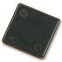
H5PS5162FFR-S6C HYNIX SEMICONDUCTOR, H5PS5162FFR-S6C Datasheet - Page 33

H5PS5162FFR-S6C
Manufacturer Part Number
H5PS5162FFR-S6C
Description
58T1896
Manufacturer
HYNIX SEMICONDUCTOR
Datasheet
1.H5PS5162FFR-S6C.pdf
(39 pages)
Specifications of H5PS5162FFR-S6C
Memory Type
SDRAM
Memory Configuration
32M X 16
Memory Case Style
FBGA
No. Of Pins
84
Operating Temperature Range
0°C To +85°C
Memory Size
512 Mbit
Voltage Vcc
1.8V
Rohs Compliant
Yes
Available stocks
Company
Part Number
Manufacturer
Quantity
Price
Company:
Part Number:
H5PS5162FFR-S6C
Manufacturer:
HYNIX
Quantity:
9 500
Company:
Part Number:
H5PS5162FFR-S6C
Manufacturer:
HYNIX
Quantity:
2 000
Company:
Part Number:
H5PS5162FFR-S6C
Manufacturer:
ST
Quantity:
40
Company:
Part Number:
H5PS5162FFR-S6C
Manufacturer:
HYNIX
Quantity:
4 000
Part Number:
H5PS5162FFR-S6C
Manufacturer:
HYNIX/海力士
Quantity:
20 000
Rev. 1.0 / July. 2008
15. The clock frequency is allowed to change during self–refresh mode or precharge power-down mode.
In case of clock frequency change during precharge power-down, a specific procedure is required as
described in section 2.9.
16. ODT turn on time min is when the device leaves high impedance and ODT resistance begins to turn on.
17. ODT turn off time min is when the device starts to turn off ODT resistance.
18. tHZ and tLZ transitions occur in the same access time as valid data transitions. Thesed parameters are
referenced to a specific voltage level which specifies when the device output is no longer driving(tHZ), or
begins driving (tLZ). Below figure shows a method to calculate the point when device is no longer driving
(tHZ), or begins driving (tLZ) by measuring the signal at two different voltages. The actual voltage mea-
surement points are not critical as long as the calculation is consistenet.
19. tRPST end point and tRPRE begin point are not referenced to a specific voltage level but specify when
the device output is no longer driving (tRPST), or begins driving (tRPRE). Below figure shows a method to
calculate these points when the device is no longer driving (tRPST), or begins driving (tRPRE). Below Fig-
ure shows a method to calculate these points when the device is no longer driving (tRPST), or begins driv-
ing (tRPRE) by measuring the signal at two different voltages. The actual voltage measurement points are
not critical as long as the calculation is consistent.
20. Input waveform timing with differential data strobe enabled MR[bit10] =0, is referenced from the input
signal crossing at the V
the input signal crossing at the V
applied to the device under test.
21. Input waveform timing with differential data strobe enabled MR[bit10]=0, is referenced from the input
signal crossing at the V
to the differential data strobe crosspoint for a falling signal applied to the device under test.
ODT turn off time max is when the bus is in high impedance. Both are measured from tAOFD.
ODT turn on time max is when the ODT resistance is fully on. Both are measured from tAOND.
tRPST end point
tHZ , tRPST end point = 2*T1-T2
tHZ
T1
IH
IH
(ac) level to the differential data strobe crosspoint for a rising signal, and from
(dc) level to the differential data strobe crosspoint for a rising signal and V
T2
IL
VOH + xmV
VOL + 1xmV
VOL + 2xmV
VOH + 2xmV
(ac) level to the differential data strobe crosspoint for a falling signal
VTT - 2xmV
VTT + 2xmV
tLZ , tRPRE begin point = 2*T1-T2
VTT + xmV
VTT -xmV
T1
T2
H5PS5162FFR series
tLZ
tRPRE begin point
Release
IL
(dc)
33


