ADG714BRU Analog Devices Inc, ADG714BRU Datasheet
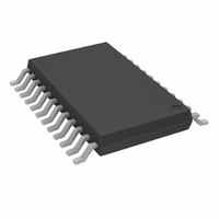
IC SWITCH OCTAL SPST 24TSSOP

ADG714BRU

Manufacturer Part Number
ADG714BRU
Description
IC SWITCH OCTAL SPST 24TSSOP
Manufacturer
Analog Devices Inc
Datasheet

Specifications of ADG714BRU

Rohs Status
RoHS non-compliant
Function
Switch
Circuit
8 x SPST - NO
On-state Resistance
4.5 Ohm
Voltage Supply Source
Single, Dual Supply
Voltage - Supply, Single/dual (±)
2.7 V ~ 5.5 V, ±1.35 V ~ 2.5 V
Current - Supply
10µA
Operating Temperature
-40°C ~ 85°C
Mounting Type
Surface Mount
Package / Case
24-TSSOP (0.173", 4.40mm Width)

Available stocks

Company
Part Number
Manufacturer
Quantity
Price
Part Number:
ADG714BRU
Manufacturer:
ADI/亚德诺
Quantity:
20 000
Part Number:
ADG714BRUZ
Manufacturer:
ADI
Quantity:
1 010
Part Number:
ADG714BRUZ
Manufacturer:
ADI
Quantity:
1
Part Number:
ADG714BRUZ
Manufacturer:
AD
Quantity:
1 020
Part Number:
ADG714BRUZ
Manufacturer:
ADI/亚德诺
Quantity:
20 000
Part Number:
ADG714BRUZ-REEL
Manufacturer:
AD
Quantity:
1 400
Part Number:
ADG714BRUZ-REEL
Manufacturer:
ADI/亚德诺
Quantity:
20 000
Part Number:
ADG714BRUZ-REEL7
Manufacturer:
ADI
Quantity:
2 000
Part Number:
ADG714BRUZ-REEL7
Manufacturer:
ADI
Quantity:
300
Part Number:
ADG714BRUZ-REEL7
Manufacturer:
ADI/亚德诺
Quantity:
20 000
a
GENERAL DESCRIPTION
The ADG714/ADG715 are CMOS, octal SPST (single-pole,
single-throw) switches controlled via either a 2- or 3-wire serial
interface. On resistance is closely matched between switches and
very flat over the full signal range. Each switch conducts equally
well in both directions and the input signal range extends to the
supplies. Data is written to these devices in the form of 8 bits,
each bit corresponding to one channel.
The ADG714 uses a 3-wire serial interface that is compatible
with SPI , QSPI, and MICROWIRE and most DSP interface
standards. The output of the shift register DOUT enables a
number of these parts to be daisy chained.
The ADG715 uses a 2-wire serial interface that is compatible
with the I
addresses, selectable from two external address pins (A0 and A1).
This allows the 2 LSBs of the 7-bit slave address to be set by
the user. A maximum of four of these devices may be connected
to the bus.
SPI and QSPI are trademarks of Motorola, Inc.
MICROWIRE is a trademark of National Semiconductor Corporation.
I
REV. B
Information furnished by Analog Devices is believed to be accurate and
reliable. However, no responsibility is assumed by Analog Devices for its
use, nor for any infringements of patents or other rights of third parties that
may result from its use. No license is granted by implication or otherwise
under any patent or patent rights of Analog Devices.
2
C is a trademark of Philips Corporation.
FEATURES
ADG714 SPI™/QSPI™/MICROWIRE™-Compatible Interface
ADG715 I
2.7 V to 5.5 V Single Supply
2.5
0.6
100 pA Leakage Currents
Octal SPST
Power-On Reset
Fast Switching Times
TTL/CMOS-Compatible
Small TSSOP Package
APPLICATIONS
Data Acquisition Systems
Communication Systems
Relay Replacement
Audio and Video Switching
2.5 V Dual Supply
2
On Resistance
On Resistance Flatness
C interface standard. The ADG715 has four hard wired
2
C™-Compatible Interface
Serially Controlled, Octal SPST Switches
On power-up of these devices, all switches are in the OFF con-
dition, and the internal registers contain all zeros.
Low power consumption and operating supply range of 2.7 V to
5.5 V make this part ideal for many applications. These parts
may also be supplied from a dual ± 2.5 V supply. The ADG714
and ADG715 are available in a small 24-lead TSSOP package.
PRODUCT HIGHLIGHTS
1. 2- or 3-wire serial interface
2. Single/dual supply operation. The ADG714 and ADG715
3. Low on resistance, typically 2.5 Ω
4. Low leakage
5. Power-on reset
6. Small 24-lead TSSOP package
One Technology Way, P.O. Box 9106, Norwood, MA 02062-9106, U.S.A.
Tel: 781/329-4700
Fax: 781/326-8703
S1
S2
S3
S4
S5
S6
S7
S8
are fully specified and guaranteed with 3 V, 5 V, and ± 2.5 V
supply rails.
SCLK DIN SYNC RESET
INPUT SHIFT
REGISTER
ADG714
FUNCTIONAL BLOCK DIAGRAMS
CMOS, Low Voltage
D1
D2
D3
D4
D5
D6
D7
D8
DOUT
ADG714/ADG715
S1
S2
S3
S4
S5
S6
S7
S8
SDA
© Analog Devices, Inc., 2002
INTERFACE
ADG715
SCL
LOGIC
A0
www.analog.com
A1
D1
D2
D3
D4
D5
D6
D7
D8
RESET

Related parts for ADG714BRU

ADG714BRU Summary of contents

Page 1

FEATURES ADG714 SPI™/QSPI™/MICROWIRE™-Compatible Interface 2 ADG715 I C™-Compatible Interface 2 5.5 V Single Supply 2.5 V Dual Supply 2.5 On Resistance 0.6 On Resistance Flatness 100 pA Leakage Currents Octal SPST Power-On Reset Fast Switching Times TTL/CMOS-Compatible ...

Page 2

ADG714/ADG715–SPECIFICATIONS Parameter ANALOG SWITCH Analog Signal Range On Resistance ( Resistance Match Between Channels (∆R On Resistance Flatness (R ) FLAT(ON) LEAKAGE CURRENTS Source OFF Leakage I (OFF) S Drain OFF Leakage I (OFF) D Channel ON ...

Page 3

SPECIFICATIONS (V DD Parameter ANALOG SWITCH Analog Signal Range On Resistance ( Resistance Match Between Channels (∆R On Resistance Flatness (R ) FLAT(ON) LEAKAGE CURRENTS Source OFF Leakage I (OFF) S Drain OFF Leakage I (OFF) ...

Page 4

ADG714/ADG715–SPECIFICATIONS DUAL SUPPLY (V = +2 Parameter ANALOG SWITCH Analog Signal Range On Resistance ( Resistance Match Between Channels (∆R On Resistance Flatness (R ) FLAT(ON) LEAKAGE CURRENTS Source OFF Leakage I (OFF) ...

Page 5

ADG714 TIMING CHARACTERISTICS Parameter Limit MIN f 30 SCLK 4 ...

Page 6

ADG714/ADG715 ADG715 TIMING CHARACTERISTICS Parameter Limit MIN MAX f 400 SCL 100 0 0 0.6 ...

Page 7

... Industrial (B Version –40°C to +85°C Storage Temperature Range . . . . . . . . . . . . –65°C to +150°C Junction Temperature . . . . . . . . . . . . . . . . . . . . . . . . . 150°C Model Temperature Range ADG714BRU –40°C to +85°C ADG715BRU –40°C to +85°C CAUTION ESD (electrostatic discharge) sensitive device. Electrostatic charges as high as 4000 V readily accumulate on the human body and test equipment and can discharge without detection ...

Page 8

ADG714/ADG715 Pin No. Mnemonic Description 1 SCLK Serial Clock Input. Data is clocked into the input shift register on the falling edge of the serial clock input. These devices can accommodate serial input rates MHz. 2 ...

Page 9

V Most positive power supply potential Most negative power supply in a dual supply SS application. In single supply applications, this should be tied to ground. I Positive Supply Current DD I Negative Supply Current SS GND Ground ...

Page 10

ADG714/ADG715 –Typical Performance Characteristics DRAIN OR SOURCE VOLTAGE – ...

Page 11

(ON (OFF) I (OFF –0.02 –0.04 0 0.5 1.0 1.5 VOLTAGE – V TPC 7. Leakage Currents as a Function of V 0.04 0. (OFF) S ...

Page 12

ADG714/ADG715 –40 –50 –60 –70 –80 –90 –100 30k 100k 1M FREQUENCY – Hz TPC 13. Crosstalk vs. Frequency +2. –2.5V SS –5 –10 –15 –20 –3 –2 ...

Page 13

The 2-wire serial bus protocol operates as follows: 1. The master initiates data transfer by establishing a START condition, which is when a high-to-low transition on the SDA line occurs while SCL is high. The following byte is the address ...

Page 14

ADG714/ADG715 APPLICATIONS Multiple Devices On One Bus Figure 6 shows four ADG715 devices on the same serial bus. Each has a different slave address since the state of their A0 and A1 pins is different. This allows each switch to ...

Page 15

SPI bus. Figure 8 illustrates the ADG739 and mul- tiple ADG714s in such a typical configuration. All devices receive the same serial clock and serial data, but only one device will receive the SYNC signal at any ...

Page 16

ADG714/ADG715 24-Lead Thin Shrink Small Outline Package [TSSOP] PIN 1 0.15 0.05 Revision History Location 11/02—Data Sheet changed from REV REV. B. Edits to FEATURES . . . . . . . . . . . . . ...

Related keywords