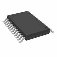
ADG714BRU Analog Devices Inc, ADG714BRU Datasheet - Page 6

ADG714BRU
Manufacturer Part Number
ADG714BRU
Description
IC SWITCH OCTAL SPST 24TSSOP
Manufacturer
Analog Devices Inc
Datasheet
1.ADG715BRUZ.pdf
(16 pages)
Specifications of ADG714BRU
Rohs Status
RoHS non-compliant
Function
Switch
Circuit
8 x SPST - NO
On-state Resistance
4.5 Ohm
Voltage Supply Source
Single, Dual Supply
Voltage - Supply, Single/dual (±)
2.7 V ~ 5.5 V, ±1.35 V ~ 2.5 V
Current - Supply
10µA
Operating Temperature
-40°C ~ 85°C
Mounting Type
Surface Mount
Package / Case
24-TSSOP (0.173", 4.40mm Width)
Available stocks
Company
Part Number
Manufacturer
Quantity
Price
Part Number:
ADG714BRU
Manufacturer:
ADI/亚德诺
Quantity:
20 000
Company:
Part Number:
ADG714BRUZ
Manufacturer:
ADI
Quantity:
1 010
Part Number:
ADG714BRUZ
Manufacturer:
ADI/亚德诺
Quantity:
20 000
Company:
Part Number:
ADG714BRUZ-REEL
Manufacturer:
AD
Quantity:
1 400
Part Number:
ADG714BRUZ-REEL
Manufacturer:
ADI/亚德诺
Quantity:
20 000
Part Number:
ADG714BRUZ-REEL7
Manufacturer:
ADI/亚德诺
Quantity:
20 000
ADG714/ADG715
ADG715 TIMING CHARACTERISTICS
Parameter
f
t
t
t
t
t
t
t
t
t
t
t
t
C
t
NOTES
1
2
3
4
Specifications subject to change without notice.
SCL
1
2
3
4
5
6
7
8
9
10
11
11
SP
See Figure 2.
A master device must provide a hold time of at least 300 ns for the SDA signal (referred to the V
SCL’s falling edge.
C
Input filtering on both the SCL and SDA inputs suppress noise spikes that are less than 50 ns.
2
b
b
4
is the total capacitance of one bus line in pF. t
SDA
SCL
t
Limit at T
400
2.5
0.6
1.3
0.6
100
0.9
0
0.6
0.6
1.3
300
20 + 0.1C
250
300
0.1C
400
50
9
CONDITION
b
START
3
t
4
b
MIN
3
, T
t
3
MAX
Figure 2. 2-Wire Serial Interface Timing Diagram
R
and t
t
10
F
measured between 0.3 V
t
6
Unit
kHz max
µs min
µs min
µs min
µs min
ns min
µs max
µs min
µs min
µs min
µs min
ns max
ns min
ns max
ns max
ns min
pF max
ns max
1
(V
DD
t
2
= 2.7 V to 5.5 V. All specifications –40 C to +85 C unless otherwise noted.)
–6–
t
11
DD
and 0.7 V
t
Conditions/Comments
SCL Clock Frequency
SCL Cycle Time
t
t
t
t
t
t
t
t
a Start Condition
t
t
t
Capacitive Load for Each Bus Line
Pulsewidth of Spike Suppressed
5
HIGH
LOW
HD, STA
SU, DAT
HD, DAT
SU, STA
SU, STO
BUF
R
F
F
, Fall Time of SDA When Receiving
, Fall Time of SDA When Transmitting
, Rise Time of Both SCL and SDA When Receiving
DD
, Bus Free Time Between a STOP Condition and
IH
, SCL Low Time
, SCL High Time
.
min of the SCL signal) in order to bridge the undefined region of
, Setup Time for Repeated Start
, Stop Condition Setup Time
, Start/Repeated Start Condition Hold Time
, Data Setup Time
, Data Hold Time
REPEATED
CONDITION
START
t
t
4
7
t
1
CONDITION
STOP
t
8
REV. B


