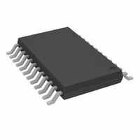
ADG714BRU Analog Devices Inc, ADG714BRU Datasheet - Page 15

ADG714BRU
Manufacturer Part Number
ADG714BRU
Description
IC SWITCH OCTAL SPST 24TSSOP
Manufacturer
Analog Devices Inc
Datasheet
1.ADG715BRUZ.pdf
(16 pages)
Specifications of ADG714BRU
Rohs Status
RoHS non-compliant
Function
Switch
Circuit
8 x SPST - NO
On-state Resistance
4.5 Ohm
Voltage Supply Source
Single, Dual Supply
Voltage - Supply, Single/dual (±)
2.7 V ~ 5.5 V, ±1.35 V ~ 2.5 V
Current - Supply
10µA
Operating Temperature
-40°C ~ 85°C
Mounting Type
Surface Mount
Package / Case
24-TSSOP (0.173", 4.40mm Width)
Available stocks
Company
Part Number
Manufacturer
Quantity
Price
Part Number:
ADG714BRU
Manufacturer:
ADI/亚德诺
Quantity:
20 000
Company:
Part Number:
ADG714BRUZ
Manufacturer:
ADI
Quantity:
1 010
Part Number:
ADG714BRUZ
Manufacturer:
ADI/亚德诺
Quantity:
20 000
Company:
Part Number:
ADG714BRUZ-REEL
Manufacturer:
AD
Quantity:
1 400
Part Number:
ADG714BRUZ-REEL
Manufacturer:
ADI/亚德诺
Quantity:
20 000
Part Number:
ADG714BRUZ-REEL7
Manufacturer:
ADI/亚德诺
Quantity:
20 000
devices on the SPI bus. Figure 8 illustrates the ADG739 and mul-
tiple ADG714s in such a typical configuration. All devices receive
the same serial clock and serial data, but only one device will
receive the SYNC signal at any one time. The ADG739 is a serially
controlled device also. One bit programmable pin of the micro-
controller is used to enable the ADG739 via SYNC2, while
another bit programmable pin is used as the chip select for the
other serial devices, SYNC1. Driving SYNC2 low enables
changes to be made to the addressed serial devices. By bringing
SYNC1 low, the selected serial device hanging from the SPI bus
will be enabled and data will be clocked into its shift register on
the falling edges of SCLK. The convenient design of the matrix
switch allows for different combinations of the four serial
devices to be addressed at any one time. If more devices need
to be addressed via one chip select line, the ADG738 is an 8-
channel device and would allow further expansion of the chip
select scheme. There may be some digital feedthrough from the
digital input lines because SCLK and DIN are permanently
connected to each device. Using a burst clock will minimize the
effects of digital feedthrough on the analog channels.
REV. B
–15–
FROM
OR DSP
CONTROLLER
Figure 8. Addressing Multiple ADG714s Using an
ADG739
SYNC2
SYNC1
SCLK
DIN
1/2 of ADG739
DA
SCLK DIN
V
DD
SYNC
ADG714/ADG715
S1A
S2A
S3A
S4A
R
R
R
R
VDD
VDD
VDD
VDD
SYNC
DIN
SCLK
SYNC
DIN
SCLK
SYNC
DIN
SCLK
SYNC
DIN
SCLK
ADG714
ADG714
OTHER
SPI
DEVICE
OTHER
SPI
DEVICE


