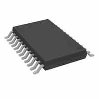
ADG714BRU Analog Devices Inc, ADG714BRU Datasheet - Page 12

ADG714BRU
Manufacturer Part Number
ADG714BRU
Description
IC SWITCH OCTAL SPST 24TSSOP
Manufacturer
Analog Devices Inc
Datasheet
1.ADG715BRUZ.pdf
(16 pages)
Specifications of ADG714BRU
Rohs Status
RoHS non-compliant
Function
Switch
Circuit
8 x SPST - NO
On-state Resistance
4.5 Ohm
Voltage Supply Source
Single, Dual Supply
Voltage - Supply, Single/dual (±)
2.7 V ~ 5.5 V, ±1.35 V ~ 2.5 V
Current - Supply
10µA
Operating Temperature
-40°C ~ 85°C
Mounting Type
Surface Mount
Package / Case
24-TSSOP (0.173", 4.40mm Width)
Available stocks
Company
Part Number
Manufacturer
Quantity
Price
Part Number:
ADG714BRU
Manufacturer:
ADI/亚德诺
Quantity:
20 000
Company:
Part Number:
ADG714BRUZ
Manufacturer:
ADI
Quantity:
1 010
Part Number:
ADG714BRUZ
Manufacturer:
ADI/亚德诺
Quantity:
20 000
Company:
Part Number:
ADG714BRUZ-REEL
Manufacturer:
AD
Quantity:
1 400
Part Number:
ADG714BRUZ-REEL
Manufacturer:
ADI/亚德诺
Quantity:
20 000
Part Number:
ADG714BRUZ-REEL7
Manufacturer:
ADI/亚德诺
Quantity:
20 000
ADG714/ADG715
TPC 15. T
TPC 14. Charge Injection vs. Source/Drain Voltage
–100
–10
–15
–20
–40
–50
–60
–70
–80
–90
10
–5
5
0
45
40
35
30
25
20
15
10
30k
–3
5
0
10
–2
V
V
100k
ON
20
TPC 13. Crosstalk vs. Frequency
DD
SS
/T
= –2.5V
= +2.5V
T
T
T
T
OFF
–1
OFF
OFF
O N
O N
30
, V
, V
, V
, V
Times vs. Temperature for ADG714
DD
DD
DD
DD
TEMPERATURE – C
0
FREQUENCY – Hz
= 5V
= 3V
VOLTAGE – V
= 5V
= 3V
40
1M
1
50
V
V
2
DD
SS
60
= GND
= +3.3V
10M
3
V
SS
V
T
V
V
A
DD
DD
SS
T
70
= GND
= 25 C
A
= 5V
= GND
= +5V
= 25 C
4
80
100M
5
–12–
GENERAL DESCRIPTION
The ADG714 and ADG715 are serially controlled, octal SPST
switches, controlled by either a 2- or 3-wire interface. Each bit
of the 8-bit serial word corresponds to one switch of the part. A
Logic 1 in the particular bit position turns on the switch, while a
Logic 0 turns the switch off. Because each switch is independently
controlled by an individual bit, this provides the option of having
any, all, or none of the switches ON.
When changing the switch conditions, a new 8-bit word is writ-
ten to the input shift register. Some of the bits may be the same
as the previous write cycle, as the user may not wish to change
the state of some switches. To minimize glitches on the output
of these switches, the part cleverly compares the state of switches
from the previous write cycle. If the switch is already in the
ON condition, and is required to stay ON, there will be minimal
glitches on the output of the switch.
POWER-ON RESET
On power-up of the device, all switches will be in the OFF con-
dition and the internal shift register is filled with zeros and will
remain so until a valid write takes place.
SERIAL INTERFACE
3-Wire Serial Interface
The ADG714 has a 3-wire serial interface (SYNC, SCLK, and
DIN), that is compatible with SPI, QSPI, MICROWIRE
interface standards and most DSPs. Figure 1 shows the tim-
ing diagram of a typical write sequence.
Data is written to the 8-bit shift register via DIN under the con-
trol of the SYNC and SCLK signals. Data may be written to
the shift register in more or less than eight bits. In each case
the shift register retains the last eight bits that were written.
When SYNC goes low, the input shift register is enabled. Data
from DIN is clocked into the shift register on the falling edge of
SCLK. Each bit of the 8-bit word corresponds to one of the eight
switches. Figure 3 shows the contents of the input shift register.
Data appears on the DOUT pin on the rising edge of SCLK
suitable for daisy chaining, delayed of course by eight bits. When
all eight bits have been written into the shift register, the SYNC
line is brought high again. The switches are updated with the
new configuration and the input shift register is disabled. With
SYNC held high, the input shift register is disabled, so further data
or noise on the DIN line will have no effect on the shift register.
SERIAL INTERFACE
2-Wire Serial Interface
The ADG715 is controlled via an I
This device is connected to the bus as a slave device (no clock is
generated by the switch).
The ADG715 has a 7-bit slave address. The five MSBs are 10010
and the two LSBs are determined by the state of the A0 and
A1 pins.
Figure 3. Input Shift Register Contents
DB7 (MSB)
S8
S7
S6
DATA BITS
S5
S4
S3
2
C-compatible serial bus.
DB0 (LSB)
S2
S1
REV. B


