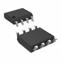
LMC567CM/NOPB National Semiconductor, LMC567CM/NOPB Datasheet - Page 2

LMC567CM/NOPB
Manufacturer Part Number
LMC567CM/NOPB
Description
IC TONE DECODER CMOS 8-SOIC
Manufacturer
National Semiconductor
Series
LMCMOS™r
Datasheet
1.LMC567CMXNOPB.pdf
(7 pages)
Specifications of LMC567CM/NOPB
Function
Tone Decoder
Number Of Circuits
1
Voltage - Supply
2 V ~ 9 V
Power (watts)
500mW
Operating Temperature
-25°C ~ 100°C
Mounting Type
Surface Mount
Package / Case
8-SOIC (3.9mm Width)
Includes
Low Supply Current Drain, Noise Rejected, Out-of-Band Signals
Operating Frequency (max)
500kHz
Operating Supply Voltage (typ)
2.5/3.3/5V
Operating Supply Voltage (min)
2V
Operating Supply Voltage (max)
9V
Operating Temp Range
-25C to 125C
Operating Temperature Classification
Commercial
Package Type
SOIC N
Mounting
Surface Mount
Pin Count
8
Supply Current
0.8mA
Lead Free Status / RoHS Status
Lead free / RoHS Compliant
Current - Supply
-
Interface
-
Lead Free Status / Rohs Status
Compliant
Other names
*LMC567CM/NOPB
Available stocks
Company
Part Number
Manufacturer
Quantity
Price
Company:
Part Number:
LMC567CM/NOPB
Manufacturer:
NSC
Quantity:
1 151
www.national.com
I4
V3
R3
I8
f
∆f
V
∆V
V8
L.D.B.W.
∆BW
f
V
Symbol
0
max
Absolute Maximum Ratings
If Military/Aerospace specified devices are required,
please contact the National Semiconductor Sales Office/
Distributors for availability and specifications.
Electrical Characteristics
Test Circuit, T
Note 1: Absolute Maximum Ratings indicate limits beyond which damage to the device may occur. Operating Ratings indicate conditions for which the device is
functional, but do not guarantee specific performance limits. Electrical Characteristics state DC and AC electrical specifications under particular test conditions which
guarantee specific performance limits. This assumes that the device is within the Operating Ratings. Specifications are not guaranteed for parameters where no limit
is given, however, the typical value is a good indication of device performance.
in
in
0
Input Voltage, Pin 3
Supply Voltage, Pin 4
Output Voltage, Pin 8
Voltage at All Other Pins
Output Current, Pin 8
Package Dissipation
Operating Temperature Range (T
in
Power Supply
Current
Input D.C. Bias
Input Resistance
Output Leakage
Center Frequency,
F
Center Frequency
Shift with Supply
Input Threshold
Input Hysteresis
Output "Sat’ Voltage
Largest Detection
Bandwidth
Bandwidth Skew
Highest Center Freq.
Input Threshold at
f
max
osc
A
÷ 2
Parameter
= 25˚C, V
s
= 5V, RtCt #2, Sw. 1 Pos. 0, and no input, unless otherwise noted.
A
)
RtCt #1, Quiescent
or Activated
RtCt #2, Measure Oscillator
Frequency and Divide by 2
Set Input Frequency Equal to f
Above, Increase Input Level Until Pin 8
Goes Low.
Starting at Input Threshold, Decrease Input
Level Until Pin 8 goes High.
Input Level
Choose RL for Specified I8
Measure F
Pos. 0, 1, and 2;
RtCt #3, Measure Oscillator Frequency and Divide by 2
Set Input Frequency Equal to f
Increase Input Level Until Pin 8 goes Low.
−25˚C to +125˚C
osc
(Note 1)
>
Vs to Gnd
Threshold
with Sw. 1 in
500 mW
Conditions
2 V
30 mA
10V
13V
p–p
2
0
max
Measured
Storage Temperature Range
Soldering Information
See AN-450 “Surface Mounting Methods and Their Effect
on Product Reliability” for other methods of soldering
surface mount devices.
Dual-In-Line Package
Small Outline Package
measured Above,
Soldering (10 sec.)
Vapor Phase (60 sec.)
Infrared (15 sec.)
V
V
V
V
V
V
V
V
V
I8 = 2 mA
I8 = 20 mA
V
V
V
s
s
s
s
s
s
s
s
s
s
s
s
= 2V
= 5V
= 9V
= 2V
= 5V
= 9V
= 2V
= 5V
= 9V
= 2V
= 5V
= 9V
Min
92
11
17
11
7
0.06
Typ
103
105
700
0.3
0.5
0.8
1.0
1.5
0.7
40
98
20
30
45
11
14
15
35
0
1
0
−55˚C to +150˚C
±
Max
0.15
100
113
0.8
1.3
2.0
27
45
15
17
1.0
260˚C
215˚C
220˚C
mVrms
mVrms
mVrms
Units
mAdc
mVdc
nAdc
%/V
kHz
Vdc
kHz
kΩ
%
%


