LMV1090TL/NOPB National Semiconductor, LMV1090TL/NOPB Datasheet - Page 5
LMV1090TL/NOPB
Manufacturer Part Number
LMV1090TL/NOPB
Description
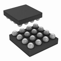
IC AMP MIC DUAL INPUT 16USMD
Manufacturer
National Semiconductor
Series
PowerWise®r
Type
Class ABr
Datasheet
1.LMV1090TLNOPB.pdf
(24 pages)
Specifications of LMV1090TL/NOPB
Output Type
2-Channel (Stereo)
Voltage - Supply
2.7 V ~ 5.5 V
Features
Differential Inputs, Microphone, Shutdown
Mounting Type
Surface Mount
Package / Case
16-MicroSMD
Lead Free Status / RoHS Status
Lead free / RoHS Compliant
Max Output Power X Channels @ Load
-
Lead Free Status / Rohs Status
Details
Other names
LMV1090TLTR


Symbol
THD+N Total Harmonic Distortion + Noise
FFNS
CMRR Common Mode Rejection Ratio
SNRI
PSRR Power Supply Rejection Ratio
Z
SNR
V
Z
e
A
A
V
Absolute Maximum Ratings
If Military/Aerospace specified devices are required,
please contact the National Semiconductor Sales Office/
Distributors for availability and specifications.
Electrical Characteristics 3.3V
Unless otherwise specified, all limits guaranteed for T
20dB, Post Amp gain = 6dB, R
V
Z
LOAD
A
Supply Voltage
Storage Temperature
Power Dissipation (Note 3)
ESD Rating (Note 4)
ESD Rating (Note 5)
Junction Temperature (T
Mounting Temperature
A
e
VBM
OUT
OUT
MR
BM
PR
IN
IN
Infrared or Convection (20 sec.)
N
M
P
CDM
E
E
Signal-to-Noise Ratio
Input Referred Noise level
Maximum Input Signal
Maximum AC Output Voltage
DC Level at Outputs
Input Impedance
Output Impedance (Differential)
Load Impedance (Out+, Out-)
Microphone Preamplifier Gain Range
Microphone Preamplifier Gain Adjustment Resolution
Post Amplifier Gain Range
Post Amplifier Gain Resolution
Far Field Noise Suppression Electrical
Signal-to-Noise Ratio Improvement Electrical
Microphone Bias Supply Voltage
Mic bias noise voltage on V
JMAX
Parameter
)
L
= 100kΩ, and C
REF
(Note
pin
6.0V
-85°C to +150°C
Internally Limited
2000V
200V
500V
150°C
235°C
10)
(Note
L
= 4.7pF, f = 1kHz pass through mode.
(Note
A
1)
= 25°C, V
1,
V
A-weighted, Audio band
V
voice band (300–3400Hz)
A-Weighted
THD+N < 1%, Pre Amp Gain = 6dB
Differential Out+, Out-
THD+N < 1%
Out+, Out-
Differential Out+ and Out-
R
C
minimum
maximum
minimum
maximum
f = 1kHz (See Test Method)
f = 300Hz (See Test Method)
f = 1kHz (See Test Method)
f = 300Hz (See Test Method)
Input Referred, Input AC grounded
f
f
input referred
I
A-Weighted, C
Note
RIPPLE
RIPPLE
BIAS
IN
OUT
LOAD
LOAD
5
DD
= 18mV
= 1.2mA
= 18V
2)
= 3.3V, V
Operating Ratings
= 217Hz (V
= 1kHz (V
Thermal Resistance
θ
Soldering Information See AN-112 “microSMD Wafers Level
Chip Scale Package.”
Supply Voltage
I
Supply Voltage (Note 8)
T
2
MIN
CV
JA
P-P
P-P
DD
≤
Conditions
(microSMD)
,
T
B
A
IN
= 10nF
RIPPLE
≤
= 18mV
RIPPLE
T
MAX
= 100mV
= 100mV
P-P
, f = 1kHz, EN = V
P-P
P-P
)
)
(Note
(Note
Typical
880
820
142
220
1.2
0.1
2.0
63
65
36
18
34
42
26
33
99
95
60
5
6
2
6
3
7
LMV1090
6)
1)
DD
(Note
2.7V
1.7V
−40°C
70°C/W
, Pre Amp gain =
Limit
1.85
2.15
820
100
1.1
0.2
1.7
2.3
2.6
3.4
10
26
18
85
80
≤
≤
7)
≤
I
www.national.com
V
2
CV
T
DD
mV
V
A
pF (max)
dB (max)
dB (max)
kΩ (min)
% (max)
dB (min)
dB (min)
dB (min)
dB (min)
(Limits)
RMS
V (max)
≤
≤
DD
V (min)
μV
μV
Units
P-P
+85°C
mV
5.5V
dB
dB
kΩ
dB
dB
dB
dB
dB
dB
dB
dB
dB
≤
Ω
RMS
RMS
(min)
(min)
5.5V
Related parts for LMV1090TL/NOPB
Image
Part Number
Description
Manufacturer
Datasheet
Request
R

Part Number:
Description:
Dual Input, Far Field Noise Suppression Microphone Amplifier
Manufacturer:
NSC [National Semiconductor]
Datasheet:

Part Number:
Description:
National Semiconductor [8-Bit D/A Converter]
Manufacturer:
National Semiconductor
Datasheet:
Part Number:
Description:
National Semiconductor [Media Coprocessor]
Manufacturer:
National Semiconductor
Datasheet:
Part Number:
Description:
Digitally Controlled Tone and Volume Circuit with Stereo Audio Power Amplifier, Microphone Preamp Stage and National 3D Sound
Manufacturer:
National Semiconductor
Datasheet:
Part Number:
Description:
Digitally Controlled Tone and Volume Circuit with Stereo Audio Power Amplifier, Microphone Preamp Stage and National 3D Sound
Manufacturer:
National Semiconductor
Datasheet:
Part Number:
Description:
AC97 Rev 2 Codec with Sample Rate Conversion and National 3D Sound
Manufacturer:
National Semiconductor
Part Number:
Description:
Manufacturer:
National Semiconductor
Datasheet:
Part Number:
Description:
Manufacturer:
National Semiconductor
Datasheet:
Part Number:
Description:
General Purpose, Low Voltage, Low Power, Rail-to-Rail Output Operational Amplifiers
Manufacturer:
National Semiconductor
Datasheet:
Part Number:
Description:
8-bit 20 MSPS flash A/D converter.
Manufacturer:
National Semiconductor
Datasheet:
Part Number:
Description:
Low Noise Quad Operational Amplifier
Manufacturer:
National Semiconductor
Datasheet:
Part Number:
Description:
Quad Differential Line Receivers
Manufacturer:
National Semiconductor
Datasheet:
Part Number:
Description:
Quad High Speed Trapezoidal? Bus Transceiver
Manufacturer:
National Semiconductor
Datasheet:
Part Number:
Description:
Dual Line Receiver
Manufacturer:
National Semiconductor
Datasheet: