LM4731TA/NOPB National Semiconductor, LM4731TA/NOPB Datasheet - Page 12
LM4731TA/NOPB
Manufacturer Part Number
LM4731TA/NOPB
Description
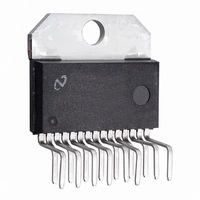
IC AMP AUDIO PWR 25W AB TO220-15
Manufacturer
National Semiconductor
Type
Class ABr
Datasheet
1.LM4731TANOPB.pdf
(16 pages)
Specifications of LM4731TA/NOPB
Output Type
2-Channel (Stereo)
Max Output Power X Channels @ Load
25W x 2 @ 8 Ohm
Voltage - Supply
20 V ~ 56 V, ±10V ~ 28 V
Features
Depop, Mute, Short-Circuit and Thermal Protection
Mounting Type
Through Hole
Package / Case
TO-220-15 (Bent and Staggered Leads)
Lead Free Status / RoHS Status
Lead free / RoHS Compliant
Other names
*LM4731TA
*LM4731TA/NOPB
LM4731TA
*LM4731TA/NOPB
LM4731TA
Available stocks
Company
Part Number
Manufacturer
Quantity
Price
Company:

Part Number:
LM4731TA/NOPB
Manufacturer:
PANASONIC
Quantity:
230


www.national.com
Application Information
To achieve a transient free power-up and power-down, the
voltage seen at the input terminals should be ideally the
same. Such a signal will be common-mode in nature, and
will be rejected by the LM4731. In Figure 3, the resistor R
serves to keep the inputs at the same potential by limiting the
voltage difference possible between the two nodes. This
should significantly reduce any type of turn-on pop, due to an
uneven charging of the amplifier inputs. This charging is
based on a specific application loading and thus, the system
designer may need to adjust these values for optimal perfor-
mance.
As shown in Figure 3, the resistors labeled R
the LM4731 off the half-supply node at the emitter of the
2N3904. But due to the input and output coupling capacitors
in the circuit, along with the negative feedback, there are two
different values of R
resistors bring up the inputs at the same rate resulting in a
popless turn-on. Adjusting these resistors values slightly
may reduce pops resulting from power supplies that ramp
extremely quick or exhibit overshoot during system turn-on.
PROPER SELECTION OF EXTERNAL COMPONENTS
Proper selection of external components is required to meet
the design targets of an application. The choice of external
component values that will affect gain and low frequency
response are discussed below.
The gain of each amplifier is set by resistors R
non-inverting configuration shown in Figure 1. The gain is
found by Equation (4) below:
For best noise performance, lower values of resistors are
used. A value of 1kΩ is commonly used for R
setting the value of R
the gain should be set no lower than 10V/V and no higher
than 50V/V. Gain settings below 10V/V may experience
A
V
BI
f
= 1 + R
, namely 10 kΩ and 200 kΩ. These
for the desired gain. For the LM4731
f
/ R
i
(V/V)
(Continued)
BI
f
and R
help bias up
i
and then
i
for the
INP
(4)
12
instability and using the LM4731 for gains higher than 50V/V
will see an increase in noise and THD.
The combination of R
pass filter. The low frequency response is determined by
these two components. The -3dB point can be found from
Equation (5) shown below:
If an input coupling capacitor is used to block DC from the
inputs as shown in Figure 4, there will be another high pass
filter created with the combination of C
using a input coupling capacitor R
bias point on the amplifier’s input terminal. The resulting
-3dB frequency response due to the combination of C
R
PHYSICAL IC MOUNTING CONSIDERATIONS
Mounting of the TO-220 package to a heat sink must be
done such that there is sufficient pressure from the mounting
screw to insure good contact with the heat sink for efficient
heat flow. Over tightening the mounting screw will cause the
TO-220 package to warp reducing contact area with the heat
sink. Less contact with the heat sink will increase the thermal
resistance from the TO-220 package case to the heat sink
(θ
possible unwanted thermal shut down activation. Extreme
over tightening of the mounting screw will cause severe
physical stress resulting in cracked die and catastrophic IC
failure. The recommended maximum mounting screw torque
is 40 inch-lbs or 3.3 foot-lbs (4.5 newton-meter).
Additionally, if the mounting screw is used to force the TO-
220 package into correct alignment with the heat sink, pack-
age stress will be increased. This increase in package stress
will result in reduced contact area with the heat sink increas-
ing die operating temperature and possible catastrophic IC
failure.
IN
CS
can be found from Equation (6) shown below:
) resulting in higher operating die temperatures and
f
IN
f
i
= 1 / (2πR
= 1 / (2πR
i
with C
i
(see Figure 1) creates a high
IN
i
C
C
i
IN
) (Hz)
IN
is needed to set the DC
) (Hz)
IN
and R
IN
. When
IN
and
(5)
(6)
Related parts for LM4731TA/NOPB
Image
Part Number
Description
Manufacturer
Datasheet
Request
R

Part Number:
Description:
National Semiconductor [8-Bit D/A Converter]
Manufacturer:
National Semiconductor
Datasheet:
Part Number:
Description:
National Semiconductor [Media Coprocessor]
Manufacturer:
National Semiconductor
Datasheet:
Part Number:
Description:
Digitally Controlled Tone and Volume Circuit with Stereo Audio Power Amplifier, Microphone Preamp Stage and National 3D Sound
Manufacturer:
National Semiconductor
Datasheet:
Part Number:
Description:
Digitally Controlled Tone and Volume Circuit with Stereo Audio Power Amplifier, Microphone Preamp Stage and National 3D Sound
Manufacturer:
National Semiconductor
Datasheet:
Part Number:
Description:
AC97 Rev 2 Codec with Sample Rate Conversion and National 3D Sound
Manufacturer:
National Semiconductor
Part Number:
Description:
Manufacturer:
National Semiconductor
Datasheet:
Part Number:
Description:
Manufacturer:
National Semiconductor
Datasheet:
Part Number:
Description:
General Purpose, Low Voltage, Low Power, Rail-to-Rail Output Operational Amplifiers
Manufacturer:
National Semiconductor
Datasheet:
Part Number:
Description:
8-bit 20 MSPS flash A/D converter.
Manufacturer:
National Semiconductor
Datasheet:
Part Number:
Description:
Low Noise Quad Operational Amplifier
Manufacturer:
National Semiconductor
Datasheet:
Part Number:
Description:
Quad Differential Line Receivers
Manufacturer:
National Semiconductor
Datasheet:
Part Number:
Description:
Quad High Speed Trapezoidal? Bus Transceiver
Manufacturer:
National Semiconductor
Datasheet:
Part Number:
Description:
Dual Line Receiver
Manufacturer:
National Semiconductor
Datasheet:
Part Number:
Description:
TTL to 10k ECL Level Translator with Latch
Manufacturer:
National Semiconductor
Datasheet: