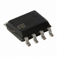
TS4871ID STMicroelectronics, TS4871ID Datasheet - Page 22

TS4871ID
Manufacturer Part Number
TS4871ID
Description
IC AMP AUDIO PWR 1W MONO 8SOIC
Manufacturer
STMicroelectronics
Type
Class ABr
Datasheet
1.TS4871IST.pdf
(28 pages)
Specifications of TS4871ID
Output Type
1-Channel (Mono)
Max Output Power X Channels @ Load
1W x 1 @ 8 Ohm
Voltage - Supply
2.5 V ~ 5.5 V
Features
Depop, Standby, Thermal Protection
Mounting Type
Surface Mount
Package / Case
8-SOIC (3.9mm Width)
Operational Class
Class-AB
Audio Amplifier Output Configuration
1-Channel Mono
Output Power (typ)
1x1@8OhmW
Audio Amplifier Function
Speaker
Total Harmonic Distortion
0.15@8Ohm@250mW%
Single Supply Voltage (typ)
3/5V
Dual Supply Voltage (typ)
Not RequiredV
Supply Current (max)
8@5VmA
Power Supply Requirement
Single
Unity Gain Bandwidth Product (typ)
2MHz
Rail/rail I/o Type
Rail to Rail Output
Power Supply Rejection Ratio
75dB
Single Supply Voltage (min)
2.5V
Single Supply Voltage (max)
5.5V
Dual Supply Voltage (min)
Not RequiredV
Dual Supply Voltage (max)
Not RequiredV
Operating Temp Range
-40C to 85C
Operating Temperature Classification
Industrial
Mounting
Surface Mount
Pin Count
8
Package Type
SOIC
Product
Class-A
Output Power
1 W
Thd Plus Noise
0.15 %
Operating Supply Voltage
3 V, 5 V
Supply Current
6 mA
Maximum Operating Temperature
+ 85 C
Mounting Style
SMD/SMT
Audio Load Resistance
8 Ohms
Input Offset Voltage
- 0.3 V to + 0.3 V
Input Signal Type
Single
Minimum Operating Temperature
- 40 C
Output Signal Type
Differential
Supply Type
Single
Supply Voltage (max)
5.5 V
Supply Voltage (min)
2.5 V
Lead Free Status / RoHS Status
Lead free / RoHS Compliant
Other names
497-2290-5
Available stocks
Company
Part Number
Manufacturer
Quantity
Price
Part Number:
TS4871ID
Manufacturer:
ST
Quantity:
20 000
Company:
Part Number:
TS4871IDT
Manufacturer:
st
Quantity:
2 486
Part Number:
TS4871IDT
Manufacturer:
ST
Quantity:
20 000
TS4871
the internal generator resistance 50k .
Then, the charge time constant for Cb is
As Cb is directly connected to the non-inverting
input (pin 2 & 3) and if we want to minimize, in
amplitude and duration, the output spike on Vout1
(pin 5), Cin must be charged faster than Cb. The
charge time constant of Cin is
Thus we have the relation
The respect of this relation permits to minimize the
pop and click noise.
Remark : Minimize Cin and Cb has a benefit on
pop and click phenomena but also on cost and
size of the application.
Example : your target for the -3dB cut off
frequency is 100 Hz. With Rin=Rfeed=22 k ,
Cin=72nF (in fact 82nF or 100nF).
With Cb=1µF, if you choose the one of the latest
two values of Cin, the pop and click phenomena at
power supply ON or standby function ON/OFF will
be very small
50 k x1µF >> 44k x100nF (50ms >> 4.4ms).
Increasing Cin value increases the pop and click
phenomena to an unpleasant sound at power
supply ON and standby function ON/OFF.
Why Cs is not important in pop and click
consideration ?
Hypothesis :
• Cs = 100µF
• Supply voltage = 5V
• Supply voltage internal resistor = 0.1
• Supply current of the amplifier Icc = 6mA
At power ON of the supply, the supply capacitor is
charged through the internal power supply
resistor. So, to reach 5V you need about five to ten
times the charging time constant of Cs ( s =
0.1xCs (s)).
Then, this time equal 50µs to 100µs << b in the
majority of application.
At power OFF of the supply, Cs is discharged by a
constant current Icc. The discharge time from 5V
to 0V of Cs is:
22/28
b = 50k xCb (s)
in = (Rin+Rfeed)xCin (s)
in << b (s)
Now, we must consider the discharge time of Cb.
At power OFF or standby ON, Cb is discharged by
a 100k
In the majority of application, Cb=1µF, then
Given :
• Load impedance : 8
• Output power @ 1% THD+N : 0.5W
• Input impedance : 10k
• Input voltage peak to peak : 1Vpp
• Bandwidth frequency : 20Hz to 20kHz (0, -3dB)
• Ambient temperature max = 50°C
• SO8 package
First of all, we must calculate the minimum power
supply voltage to obtain 0.5W into 8 . With curves
in fig. 15, we can read 3.5V. Thus, the power
supply voltage value min. will be 3.5V.
Following
equation
with 3.5V we have Pdissmax=0.31W.
Refer to power derating curves (fig. 20), with
0.31W the maximum ambient temperature will be
100°C. This last value could be higher if you follow
the example layout shown on the demoboard
(better dissipation).
The gain of the amplifier in flat region will be:
We have Rin > 10k . Let's take Rin = 10k , then
Rfeed = 28.25k . We could use for Rfeed = 30k
in normalized value and the gain will be Gv = 6.
In lower frequency we want 20 Hz (-3dB cut off
frequency). Then:
So, we could use for Cin a 1µF capacitor value
b
b
Disch
Disch
Power amplifier design examples
G
V
=
300ms >> t
3xCbx100k
resistor. So the discharge time is about
V
-------------------- - =
V
OUTP P
t
the
I N P P
D i s ch C s
Pdiss
maximum
dischCs
max
=
2 2 R
----------------------------------- - = 5.65
(s).
------------- - = 83 ms
5Cs
Icc
V
.
min.
I N P P
2
L
Vcc
2
P
R
power
OUT
L
2
(
W
)
dissipation


