LM4928TLX/NOPB National Semiconductor, LM4928TLX/NOPB Datasheet
LM4928TLX/NOPB
Specifications of LM4928TLX/NOPB


Related parts for LM4928TLX/NOPB


LM4928TLX/NOPB Summary of contents
Page 1
... The LM4928 contains advanced pop & click circuitry which eliminates noises which would otherwise occur during turn-on and turn-off transitions. Boomer ® registered trademark of National Semiconductor Corporation. © 2006 National Semiconductor Corporation Key Specifications j Improved PSRR at 217Hz j Output Power at 5.0V j Output Power at 3 ...
Page 2
Typical Application FIGURE 1. Typical Audio Amplifier Application Circuit www.national.com 2 201600B7 ...
Page 3
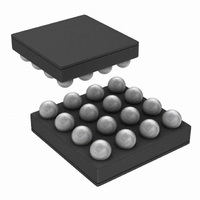
Connection Diagrams LLP Package Top View Order Number LM4928SD See NS Package Number SDA14A micro SMD Package Top View Order Number LM4928TL See NS Package Number TLA16 ...
Page 4
... Absolute Maximum Ratings If Military/Aerospace specified devices are required, please contact the National Semiconductor Sales Office/ Distributors for availability and specifications. Supply Voltage Storage Temperature Input Voltage Power Dissipation (Note 3) ESD Susceptibility (Note 4) ESD Susceptibility (Note 5) Junction Temperature Thermal Resistance Electrical Characteristics V ...
Page 5
Electrical Characteristics V The following specifications apply for V 25˚C. (Continued) Symbol Parameter P Output Power o THD+N Total Harmonic Distortion + Noise PSRR Power Supply Rejection Ratio CMRR Common-Mode Rejection Ratio V Output Offset OS V Shutdown Voltage Input ...
Page 6
Typical Performance Characteristics THD+N vs Frequency V = 2.6V 4Ω THD+N vs Frequency 4Ω THD+N vs Frequency 4Ω www.national.com ...
Page 7
Typical Performance Characteristics THD+N vs Output Power V = 2.6V 4Ω THD+N vs Output Power 4Ω THD+N vs Output Power 4Ω (Note ...
Page 8
Typical Performance Characteristics PSRR vs Common Mode Voltage 8Ω 217Hz DD L PSRR vs Frequency 8Ω Input Terminated to GND 500kHz Output Power vs ...
Page 9
Typical Performance Characteristics CMRR vs Frequency 8Ω Crosstalk vs Frequency 8Ω Top = Vin Left driven, Vout Right measured Bot = Vin Right driven, ...
Page 10
Typical Performance Characteristics Power Dissipation vs Output Power Noise Floor Output Power vs Load Resistance www.national.com (Note 10) (Continued) Power Dissipation vs Output Power 201600C6 201600C2 Clipping Voltage vs Supply Voltage 201600C4 ...
Page 11
Typical Performance Characteristics Power Derating Curve (SD Package 1kHz 8Ω Power Derating Curve (TL Package 1kHz 8Ω (Note 10) (Continued) Power Derating Curve (SD Package 20160068 ...
Page 12
... Demonstration Board Layout section. Further detailed and specific information concerning PCB layout, fabrication, and mounting an LLP package is available from National Semiconductor’s package Engineering Group un- der application note AN1187. PCB LAYOUT AND SUPPLY REGULATION CONSIDERATIONS FOR DRIVING 4Ω LOADS Power dissipated by a load is a function of the voltage swing across the load and the load’ ...
Page 13
Application Information (2π Single-Ended DMAX DD L However, a direct consequence of the increased power de- livered to the load by a bridge amplifier is an increase in internal power dissipation ...
Page 14
Application Information Special care must be taken to match the values of the input resistors (R and R ) and (R and Because of the balanced nature of differential amplifiers, resistor matching differences can result in ...
Page 15
LM4928 Demo Board Schematic 15 20160073 www.national.com ...
Page 16
LM4928 LLP Demo Board Artwork Top Silkscreen Bottom Layer and Ground Plane www.national.com 20160009 20160007 16 Top Layer 20160008 ...
Page 17
LM4928 microSMD Board Artwork Top Silkscreen Middle Layer 20160013 Bottom Layer and Ground Plane 20160010 17 Top Layer 20160012 20160011 www.national.com ...
Page 18
Revision History Rev 1.0 1.1 1.2 1.3 1.4 1.5 1.6 1.7 1.8 1.9 2.0 2.1 2.2 www.national.com Date 7/13/05 Input first set of edits. 10/3/05 More edits input. 10/10/05 Input few text edits. 10/25/04 Added the Typ Perf section. 11/02/05 ...
Page 19
Physical Dimensions inches (millimeters) unless otherwise noted X1 = 1.970 LLP Package Order Number LM4928SD NS Package Number SDA14A 16–bump micro SMD Order Number LM4928TL NS Package Number TLA1611A ± ± 0.03 1.970 0.03 0.600 19 ...
Page 20
... BANNED SUBSTANCE COMPLIANCE National Semiconductor manufactures products and uses packing materials that meet the provisions of the Customer Products Stewardship Specification (CSP-9-111C2) and the Banned Substances and Materials of Interest Specification (CSP-9-111S2) and contain no ‘‘Banned Substances’’ as defined in CSP-9-111S2. ...