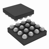
LM4928TLX/NOPB National Semiconductor, LM4928TLX/NOPB Datasheet - Page 4

LM4928TLX/NOPB
Manufacturer Part Number
LM4928TLX/NOPB
Description
IC AMP AUDIO PWR 2.2W AB 16USMD
Manufacturer
National Semiconductor
Series
Boomer®r
Type
Class ABr
Datasheet
1.LM4928TLNOPB.pdf
(20 pages)
Specifications of LM4928TLX/NOPB
Output Type
2-Channel (Stereo)
Max Output Power X Channels @ Load
2.2W x 2 @ 4 Ohm
Voltage - Supply
2.4 V ~ 5.5 V
Features
Depop, Differential Inputs, Shutdown, Thermal Protection
Mounting Type
Surface Mount
Package / Case
16-MicroSMD
Operational Class
Class-AB
Audio Amplifier Output Configuration
2-Channel Stereo
Output Power (typ)
1.5x2@8OhmW
Audio Amplifier Function
Speaker
Total Harmonic Distortion
0.04@8Ohm@1W%
Single Supply Voltage (typ)
3/5V
Dual Supply Voltage (typ)
Not RequiredV
Power Supply Requirement
Single
Rail/rail I/o Type
No
Power Supply Rejection Ratio
90dB
Single Supply Voltage (min)
2.4V
Single Supply Voltage (max)
5.5V
Dual Supply Voltage (min)
Not RequiredV
Dual Supply Voltage (max)
Not RequiredV
Operating Temp Range
-40C to 85C
Operating Temperature Classification
Industrial
Mounting
Surface Mount
Pin Count
16
Package Type
uSMD
For Use With
LM4928TLBD - BOARD EVALUATION LM4928TL
Lead Free Status / RoHS Status
Lead free / RoHS Compliant
Other names
LM4928TLX
www.national.com
I
I
P
THD+N
PSRR
CMRR
V
V
V
SNR
T
I
I
DD
SD
DD
SD
Symbol
Symbol
WU
o
OS
SDIH
SDIL
Absolute Maximum Ratings
If Military/Aerospace specified devices are required,
please contact the National Semiconductor Sales Office/
Distributors for availability and specifications.
Electrical Characteristics V
The following specifications apply for V
Electrical Characteristics V
The following specifications apply for V
Supply Voltage
Storage Temperature
Input Voltage
Power Dissipation (Note 3)
ESD Susceptibility (Note 4)
ESD Susceptibility (Note 5)
Junction Temperature
Thermal Resistance
Quiescent Power Supply Current
Shutdown Current
Output Power
Total Harmonic Distortion + Noise
Power Supply Rejection Ratio
Common-Mode Rejection Ratio
Output Offset
Shutdown Voltage Input High
Shutdown Voltage Input Low
Signal-to-Noise Ratio
Wake-up time from Shutdown
Quiescent Power Supply Current
Shutdown Current
Parameter
Parameter
DD
DD
−0.3V to V
= 5V, A
= 3V, A
Internally Limited
−65˚C to +150˚C
DD
DD
V
V
(Both amplifiers)
V
(Both amplifiers)
V
V
(Both amplifiers)
V
(Both amplifiers)
THD = 1% (max); f = 1 kHz
THD = 10% (max); f = 1 kHz
P
V
f = 217Hz, V
V
P
Cbypass = 1µF
(Note 2)
IN
IN
SHUTDOWN
o
ripple
IN
O
IN
IN
SHUTDOWN
LM4928SD, R
LM4928SD, R
R
R
V
= 1 Wrms; f = 1kHz
V
= 5V
= 1W, f = 1kHz
= 3V
= 0V, R
DD
= 0V, no load
= 0V, R
= 0V
= 0V, no load
f = 217Hz (Note 8)
f = 1kHz (Note 8)
L
L
= 1, and 8Ω load unless otherwise specified. Limits apply for T
= 1, and 8Ω load unless otherwise specified. Limits apply for T
= 8Ω
= 8Ω
= 200mV sine p-p
2000V
150˚C
+0.3V
200V
6.0V
L
L
(Notes 1, 2)
Conditions
Conditions
= GND
= GND
CM
(Notes 1, 2)
= 8Ω
= 8Ω
4
= 200mV
L
L
= 4Ω (Note 9)
= 4Ω (Note 9)
Operating Ratings
Soldering Information
See AN-1187
Temperature Range
Supply Voltage
θ
θ
T
JA
JA
MIN
pp
(SD)
(micro SMD)
≤ T
A
≤ T
MAX
(Note 6)
Typical
(Note 6)
Typical
3.5
3.5
0.1
0.04
105
0.1
1.8
1.2
2.2
1.5
90
90
70
13
4
4
4
LM4928
LM4928
(Note 7)
(Note 7)
Limit
Limit
7.5
1.0
1.0
1.4
0.4
50
18
1
−40˚C ≤ T
2.4V ≤ V
A
A
= 25˚C.
= 25˚C.
mA (max)
mV (max)
µA (max)
DD
µA (max)
dB (min)
(Limits)
(Limits)
A
Units
Units
50˚C/W
74˚C/W
mA
≤ 85˚C
dB
dB
ms
≤ 5.5V
W
W
%
V
V


