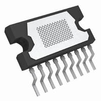
TDA1519CSP/N3C,118 NXP Semiconductors, TDA1519CSP/N3C,118 Datasheet - Page 3

TDA1519CSP/N3C,118
Manufacturer Part Number
TDA1519CSP/N3C,118
Description
IC AMP AUDIO PWR 22W MONO B 9SIL
Manufacturer
NXP Semiconductors
Type
Class Br
Datasheet
1.TDA1519CN3112.pdf
(21 pages)
Specifications of TDA1519CSP/N3C,118
Output Type
1-Channel (Mono) or 2-Channel (Stereo)
Package / Case
9-SIL (SMT Bent Leads)
Max Output Power X Channels @ Load
22W x 1 @ 4 Ohm; 11W x 2 @ 2 Ohm
Voltage - Supply
6 V ~ 17.5 V
Features
Depop, Mute, Short-Circuit and Thermal Protection, Standby
Mounting Type
Through Hole
Product
Class-B
Output Power
22 W
Available Set Gain
46 dB
Thd Plus Noise
0.1 %
Operating Supply Voltage
14.4 V
Maximum Power Dissipation
25000 mW
Maximum Operating Temperature
+ 150 C
Mounting Style
SMD/SMT
Audio Load Resistance
4 Ohms
Input Signal Type
Differential or Single
Output Signal Type
Differential, Single
Supply Type
Single
Supply Voltage (max)
17.5 V
Supply Voltage (min)
6 V
Operational Class
Class-B
Output Power (typ)
22x1@4Ohm/11x2@2OhmW
Audio Amplifier Function
Speaker
Total Harmonic Distortion
0.1@4Ohm@1W%
Single Supply Voltage (typ)
14.4V
Dual Supply Voltage (typ)
Not RequiredV
Power Supply Requirement
Single
Power Dissipation
25W
Rail/rail I/o Type
No
Single Supply Voltage (min)
6V
Single Supply Voltage (max)
17.5V
Dual Supply Voltage (min)
Not RequiredV
Dual Supply Voltage (max)
Not RequiredV
Mounting
Surface Mount
Pin Count
9 +Tab
Lead Free Status / RoHS Status
Lead free / RoHS Compliant
Lead Free Status / RoHS Status
Lead free / RoHS Compliant, Lead free / RoHS Compliant
Other names
935284474118
TDA1519CSP/N3C-T
TDA1519CSP/N3C-T
TDA1519CSP/N3C-T
TDA1519CSP/N3C-T
Philips Semiconductors
QUICK REFERENCE DATA
2004 Jan 28
Supply
V
I
I
I
I
Inputs
Stereo application
P
V
BTL application
P
SVRR
T
ORM
q(tot)
stb
sw(on)
Z
j
P
o
cs
n(o)(rms)
o
22 W BTL or 2
stereo power amplifier
i
V
SYMBOL
OO
supply voltage
repetitive peak output current
total quiescent current
standby current
switch-on current
input impedance
output power
channel separation
noise output voltage (RMS value)
output power
supply voltage ripple rejection
DC output offset voltage
junction temperature
11 W
PARAMETER
operating
non-operating
load dump protected
BTL
stereo
THD = 10 %
THD = 10 %; R
R
S
R
R
f
f
i
i
= 0
L
L
= 100 Hz
= 1 to 10 kHz
3
= 4
= 2
CONDITIONS
L
= 4
6.0
25
50
40
34
48
MIN.
14.4
40
0.1
6
11
150
22
TYP.
Product specification
TDA1519C
17.5
30
45
4
80
100
40
250
150
MAX.
V
V
V
A
mA
k
k
W
W
dB
W
dB
dB
mV
UNIT
C
A
A
V


