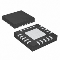
MAX3861ETG+ Maxim Integrated Products, MAX3861ETG+ Datasheet - Page 2

MAX3861ETG+
Manufacturer Part Number
MAX3861ETG+
Description
IC AMP POST W/AGC 24-TQFN-EP
Manufacturer
Maxim Integrated Products
Type
Postamplifierr
Datasheet
1.MAX3861ETG.pdf
(13 pages)
Specifications of MAX3861ETG+
Applications
Optical Networks
Mounting Type
Surface Mount
Package / Case
24-TQFN Exposed Pad
Operating Supply Voltage
3.3 V
Supply Current
94 mA
Operating Temperature Range
+ 150 C
Mounting Style
SMD/SMT
Number Of Channels
1
Power Dissipation
1350 mW
Lead Free Status / RoHS Status
Lead free / RoHS Compliant
ABSOLUTE MAXIMUM RATINGS
Supply Voltage ......................................................-0.5V to +4.0V
Voltage at IN+, IN- ..........................(V
Voltage at CZ+, CZ-, CG+,
Voltage at SC, SD, EN, TH,
CML Input Current at IN+, IN-.............................................25mA
2.7Gbps Post Amp with Automatic Gain Control
ELECTRICAL CHARACTERISTICS
(V
Stresses beyond those listed under “Absolute Maximum Ratings” may cause permanent damage to the device. These are stress ratings only, and functional
operation of the device at these or any other conditions beyond those indicated in the operational sections of the specifications is not implied. Exposure to
absolute maximum rating conditions for extended periods may affect device reliability.
2
Supply Current
Power-Supply Noise Rejection
Input Data Rate
Input Resistance
Input Return Loss
Input Common-Mode Level
Input-Referred Noise
Input Voltage Range
Maximum Differential Input
Voltage for Linear Operation
Output Resistance
Output Return Loss
Output Common-Mode Level
Maximum Differential Output
Offset
CC
CG-, CD+, CD- ............................(V
OSM, V
_______________________________________________________________________________________
= +3.0V to +3.6V, T
REF
PARAMETER
, RSSI ....................................-0.5V to (V
A
= -40°C to +85°C. Typical values are at V
SYMBOL
I
CC
CC
CC
PSNR
R
R
V
OUT
- 1.5V) to (V
- 3.5V) to (V
IN
IN
RSSI and SD enabled
(Notes 2, 3)
RSSI and SD disabled
(Notes 2, 3)
V
f
V
Single-ended to V
≤2.7GHz
2.7GHz to 4.0GHz
Up to 6GHz at max gain, C
Differential
0.9 ≤ linearity ≤ 1.1
Single-ended to V
≤2.7GHz
2.7GHz to 4.0GHz
R
V
R
(Note 5)
V
R
(Note 5)
NOISE
NOISE
SC
L
SC
L
SC
L
= 50Ω to V
= 50Ω to V
= 50Ω to V
CC
CC
CC
= 2V (Note 4)
= 0,
= 2V,
≤ 10MHz,
+ 0.5V)
+ 0.5V)
+ 0.5V)
= 100mV
CC
CC
CC
CONDITIONS
P-P
CC
CC
,
CC
CML Output Current at OUT+, OUT- ..................................25mA
Continuous Power Dissipation T
Storage Temperature Range .............................-55°C to +150°C
Operating Junction Temperature Range ...........-55°C to +150°C
Lead Temperature (soldering, 10s) .................................+300°C
(24-Pin QFN and 24-Pin Thin QFN)
(derate 20.8mW/°C above +85°C ...................................1.35W
= +3.3V and T
CZ
At minimum gain
At maximum gain
At minimum gain
At maximum gain
V
V
V
V
V
V
6mV
700mV
700mV
1200mV
6mV
700mV
700mV
1200mV
IN
IN
SC
SC
SC
SC
= 0.1µF
= 1000mV
= 10mV
= 0
= 2V
= 0
= 2V
P-P
P-P
P-P
P-P
P-P
P-P
≤ V
≤ V
P-P
P-P
A
≤ V
≤ V
IN
IN
P-P
= +25°C, unless otherwise noted.) (Note 1)
≤
IN
≤
IN
P-P
≤
≤
V
MIN
0.3
CC
40
40
6
A
-
= +85°C
V
V
TYP
0.28
0.26
0.13
±5.5
650
700
±11
2.7
CC
25
15
11
CC
72
94
57
78
35
50
21
50
16
±3
±8
-
-
MAX
1200
0.35
V
112
±14
±28
86
69
94
60
CC
60
mV
UNITS
mV
mV
Gbps
mA
mV
dB
dB
dB
Ω
Ω
V
V
RMS
P-P
P-P


