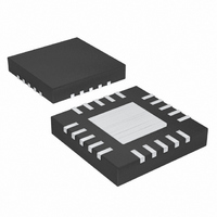
MAX3861ETG+ Maxim Integrated Products, MAX3861ETG+ Datasheet - Page 4

MAX3861ETG+
Manufacturer Part Number
MAX3861ETG+
Description
IC AMP POST W/AGC 24-TQFN-EP
Manufacturer
Maxim Integrated Products
Type
Postamplifierr
Datasheet
1.MAX3861ETG.pdf
(13 pages)
Specifications of MAX3861ETG+
Applications
Optical Networks
Mounting Type
Surface Mount
Package / Case
24-TQFN Exposed Pad
Operating Supply Voltage
3.3 V
Supply Current
94 mA
Operating Temperature Range
+ 150 C
Mounting Style
SMD/SMT
Number Of Channels
1
Power Dissipation
1350 mW
Lead Free Status / RoHS Status
Lead free / RoHS Compliant
ELECTRICAL CHARACTERISTICS (continued)
(V
2.7Gbps Post Amp with Automatic Gain Control
(V
4
Note 5: See the Distribution of Differential Output Offset (Worst-Case Conditions) graph in the Typical Operating Characteristics.
Note 6: Characterized with a 675Mbps 1-0 pattern.
Note 7: Measurements are taken over an input signal range of 16dB.
Note 8: Deterministic jitter is defined as the arithmetic sum of PWD (pulse-width distortion) and PDJ (pattern-dependent jitter).
Note 9: The typical input resistance of the SC pin is 40kΩ.
Note 10: AGC loop time constant is measured with a 20dB change in the input and V
Note 11: SD deassert time depends on the AGC loop time constant set by C
Note 12: SD accuracy is defined as the part-to-part variation of the SD threshold at a fixed R
Note 13: See the Distribution of SD Hysteresis (Worst-Case Conditions) graph in the Typical Operating Characteristics.
Note 14: Measurements are taken over an input signal range of 20dB.
CC
CC
1000
900
800
700
600
500
400
300
200
100
100
95
90
85
80
75
70
65
60
55
50
_______________________________________________________________________________________
= +3.0V to +3.6V, T
= +3.3V, T
-40
0
SUPPLY CURRENT vs. TEMPERATURE
EN = GND
EN = V
Deterministic jitter is the difference between total jitter and random jitter, with system jitter calibrated out. It is measured
with a 2
C
200
CG
-10
vs. INPUT AMPLITUDE
CC
INPUT AMPLITUDE (mV
OUTPUT AMPLITUDE
of 0.022µF connected between CG+ and CG-, a typical AGC loop time constant of 760µs is achieved.
A
400
TEMPERATURE (°C)
7
= +25°C, unless otherwise noted.)
- 1PRBS, and 80CIDs with DC-coupled outputs.
V
V
20
SC
SC
600
2
= GND
= 2.0V
23
A
EXCLUDES OUTPUT
LOAD CURRENTS
V
V
- 1PRBS AT 2.7Gbps
= -40°C to +85°C. Typical values are at V
IN
SC
800
= 1200mV
= 0
50
P-P
)
1000
P-P
80
1200
25
20
15
10
5
0
3.0
DISTRIBUTION OF SD HYSTERESIS
EYE DIAGRAM, MINIMUM INPUT
3.5
(WORST-CASE CONDITIONS)
4.0
SD HYSTERESIS (dB)
4.5
V
2
23
IN
76ps/div
= 6mV
- 1PRBS
5.0
CC
5.5
P-P
Typical Operating Characteristics
= +3.3V and T
V
V
V
T
MEAN = 4.52dB
σ = 0.79dB
6.0
A
CC
SC
IN
= -40°C
= 2mV
= 2.0V
= 3.0V
6.5
CG
P-P
.
7.0
7.5
SC
A
= +25°C, unless otherwise noted.) (Note 1)
held constant. With an external capacitor
TH
20
18
16
14
12
10
8
6
4
2
0
value.
1
EYE DIAGRAM, MAXIMUM INPUT
DETERMINISTIC JITTER
vs. INPUT AMPLITUDE
INPUT AMPLITUDE (mV
10
V
2
IN
23
76ps/div
= 1200mV
- 1PRBS
100
P-P
P-P
1000
)
10,000


