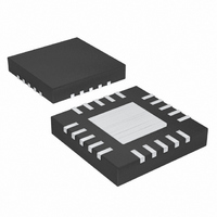
MAX3861ETG+ Maxim Integrated Products, MAX3861ETG+ Datasheet - Page 7

MAX3861ETG+
Manufacturer Part Number
MAX3861ETG+
Description
IC AMP POST W/AGC 24-TQFN-EP
Manufacturer
Maxim Integrated Products
Type
Postamplifierr
Datasheet
1.MAX3861ETG.pdf
(13 pages)
Specifications of MAX3861ETG+
Applications
Optical Networks
Mounting Type
Surface Mount
Package / Case
24-TQFN Exposed Pad
Operating Supply Voltage
3.3 V
Supply Current
94 mA
Operating Temperature Range
+ 150 C
Mounting Style
SMD/SMT
Number Of Channels
1
Power Dissipation
1350 mW
Lead Free Status / RoHS Status
Lead free / RoHS Compliant
Figure 1 is a functional diagram of the MAX3861 auto-
matic gain-control amplifier. The MAX3861 is divided
into three sections: main signal path, input signal
detection, and output signal detection.
The main signal path consists of variable gain ampli-
fiers with CML output levels and an offset-cancellation
loop. This configuration allows for overall gains from
-9.5dB to 43.5dB.
The offset-cancellation loop partially reduces additional
offset at the input. In communications systems using
NRZ data with a 50% duty cycle, pulse-width distortion
present in the signal or generated by the transimped-
ance amplifier appears as input offset and is partially
removed by the offset-cancellation loop. An external
capacitor is required between CZ+ and CZ- to com-
pensate the offset-cancellation loop and determine the
lower 3dB frequency of the signal path.
The input signal detection circuitry consists of variable
gain amplifiers and threshold voltages. Input signal
detection information is compared to an internal refer-
ence and creates the RSSI voltage and an internal ref-
erence signal. The signal detect (SD) circuitry indicates
when the input signal is below the programmed thresh-
old by comparing a voltage proportional to the RSSI
signal with internally generated control voltages. The
SD threshold is set by a control voltage developed
across the external TH resistor (R
ages, V
detect assert and deassert levels. To prevent SD chat-
ter in the region of the programmed threshold, 2.8dB to
6.3dB of hysteresis is built into the SD assert/deassert
function. Thus, once asserted, SD is not deasserted
until sufficient gain is retained. When input signal
detection (SD and RSSI) is not required, connect EN to
a TTL low to power down this circuitry.
2.7Gbps Post Amp with Automatic Gain Control
ASSERT
and V
_______________________________________________________________________________________
Input Signal Detection and
Detailed Description
Offset-Cancellation Loop
DEASSERT
Main Signal Path
TH
, define the signal
). Two control volt-
SD Circuitry
Output amplitude typically can be adjusted from
400mV
(0V to 2.0V) to the SC pin. See the Output Signal
Amplitude vs. SC Pin Voltage graph in the Typical
Operating Characteristics. Connect the V
to the SC pin for maximum output amplitude. The output
signal monitor pin provides a DC voltage linearly pro-
portional to the output signal.
The SD threshold is programmed by an external resis-
tor, R
The circuit is designed to have approximately 4.5dB of
hysteresis over the full range. See the Signal Detect
Threshold vs. R
Characteristics for proper sizing.
Figure 1. Functional Diagram
RSSI
CD+
CD-
TH
P-P
IN+
IN-
, between the range of 2mV
to 920mV
EN
V
CC
TH
P-P
graph in the Typical Operating
MAIN SIGNAL PATH
MAX3861
Program the SD Threshold
Output Signal Monitor and
CZ+
by applying a control voltage
TH
Design Procedure
CZ-
R
TH
SD CIRCUITRY
Amplitude Control
CONTROL
OUTPUT
DETECT
SIGNAL
BLOCK
AND
P-P
GND
REF
to 100mV
OUT+
OUT-
pin (2.0V)
OSM
SC
V
CG+
CG-
SD
REF
P-P
7
.


