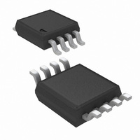
LMV393MMX/NOPB National Semiconductor, LMV393MMX/NOPB Datasheet - Page 11

LMV393MMX/NOPB
Manufacturer Part Number
LMV393MMX/NOPB
Description
IC COMP TINY DUAL LOW V 8-MSOP
Manufacturer
National Semiconductor
Type
General Purposer
Datasheet
1.LMV331M5XNOPB.pdf
(20 pages)
Specifications of LMV393MMX/NOPB
Number Of Elements
2
Output Type
CMOS, Open-Collector, TTL
Voltage - Supply
2.7 V ~ 5.5 V
Mounting Type
Surface Mount
Package / Case
8-TSSOP, 8-MSOP (0.118", 3.00mm Width)
Leaded Process Compatible
Yes
Rohs Compliant
Yes
Peak Reflow Compatible (260 C)
Yes
Lead Free Status / RoHS Status
Lead free / RoHS Compliant
Other names
LMV393MMX
LMV393MMXTR
LMV393MMXTR
Available stocks
Company
Part Number
Manufacturer
Quantity
Price
Company:
Part Number:
LMV393MMX/NOPB
Manufacturer:
IDT
Quantity:
6 246
Part Number:
LMV393MMX/NOPB
Manufacturer:
TI/德州仪器
Quantity:
20 000
NEGATIVE PEAK DETECTOR
For the negative detector, the output transistor of the com-
parator acts as a low impedance current sink. The only dis-
charge path will be the 1 MΩ resistor and any load impedance
used. Decay time is changed by varying the 1 MΩ resistor
DRIVING CMOS AND TTL
The comparator's output is capable of driving CMOS and TTL
Logic circuits.
FIGURE 9. Negative Peak Detector
FIGURE 8. Positive Peak Detector
FIGURE 10. Driving CMOS
10008005
10008018
10008017
11
AND GATES
The comparator can be used as three input AND gate. The
operation of the gate is as follow:
The resistor divider at the inverting input establishes a refer-
ence voltage at that node. The non-inverting input is the sum
of the voltages at the inputs divided by the voltage dividers.
The output will go high only when all three inputs are high,
casing the voltage at the non-inverting input to go above that
at inverting input. The circuit values shown work for a "0"
equal to ground and a "1" equal to 5V.
The resistor values can be altered if different logic levels are
desired. If more inputs are required, diodes are recommend-
ed to improve the voltage margin when all but one of the
inputs are high.
OR GATES
A three input OR gate is achieved from the basic AND gate
simply by increasing the resistor value connected from the
inverting input to V
A logic "1" at any of the inputs will produce a logic "1" at the
output.
FIGURE 11. Driving TTL
FIGURE 12. AND Gate
cc
, thereby reducing the reference voltage.
www.national.com
10008006
10008011


