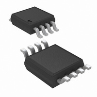
LMV393MMX/NOPB National Semiconductor, LMV393MMX/NOPB Datasheet - Page 3

LMV393MMX/NOPB
Manufacturer Part Number
LMV393MMX/NOPB
Description
IC COMP TINY DUAL LOW V 8-MSOP
Manufacturer
National Semiconductor
Type
General Purposer
Datasheet
1.LMV331M5XNOPB.pdf
(20 pages)
Specifications of LMV393MMX/NOPB
Number Of Elements
2
Output Type
CMOS, Open-Collector, TTL
Voltage - Supply
2.7 V ~ 5.5 V
Mounting Type
Surface Mount
Package / Case
8-TSSOP, 8-MSOP (0.118", 3.00mm Width)
Leaded Process Compatible
Yes
Rohs Compliant
Yes
Peak Reflow Compatible (260 C)
Yes
Lead Free Status / RoHS Status
Lead free / RoHS Compliant
Other names
LMV393MMX
LMV393MMXTR
LMV393MMXTR
Available stocks
Company
Part Number
Manufacturer
Quantity
Price
Company:
Part Number:
LMV393MMX/NOPB
Manufacturer:
IDT
Quantity:
6 246
Part Number:
LMV393MMX/NOPB
Manufacturer:
TI/德州仪器
Quantity:
20 000
V
TCV
I
I
V
A
V
I
I
t
t
B
OS
O
S
PHL
PLH
Symbol
Symbol
OS
CM
V
sat
5V DC Electrical Characteristics
Unless otherwise specified, all limits guaranteed for T
5V AC Electrical Characteristics
T
Note 1: Absolute Maximum Ratings indicate limits beyond which damage to the device may occur. Operating Ratings indicate conditions for which the device is
intended to be functional, but specific performance is not guaranteed. For guaranteed specifications and the test conditions, see the Electrical characteristics.
Note 2: Human Body Model, applicable std. MIL-STD-883, Method 3015.7. Machine Model, applicable std. JESD22-A115-A (ESD MM std. of JEDEC)
Field-Induced Charge-Device Model, applicable std. JESD22-C101-C (ESD FICDM std. of JEDEC).
Note 3: The maximum power dissipation is a function of T
P
Note 4: Typical values represent the most likely parametric norm as determined at the time of characterization. Actual typical values may vary over time and will
also depend on the application and configuration. The typical values are not tested and are not guaranteed on shipped production material.
Note 5: All limits are guaranteed by testing or statistical analysis.
D
J
OS
= (T
= 25°C, V
J(MAX)
Input Offset Voltage
Input Offset Voltage Average Drift
Input Bias Current
Input Offset Current
Input Voltage Range
Voltage Gain
Saturation Voltage
Output Sink Current
Supply Current
Output Leakage Current
Propagation Delay (High to Low)
Propagation Delay (Low to High)
- T
+
A
)/θ
= 5V, R
JA
. All numbers apply for packages soldered directly onto a PC board.
L
Parameter
Parameter
= 5.1 kΩ, V
−
= 0V.
I
V
LMV331
LMV393
Both Comparators
LMV339
All four Comparators
Input Overdrive = 10 mV
Input Overdrive = 100 mV
Input Overdrive = 10 mV
Input Overdrive = 100 mV
SINK
J(MAX)
O
≤
≤
, θ
1.5V
J
JA
= 25°C, V
4 mA
. The maximum allowable power dissipation at any ambient temperature is
Conditions
Conditions
+
3
= 5V, V
−
= 0V. Boldface limits apply at the temperature extremes.
(Note 5)
(Note 5)
Min
Min
20
(Note 4)
(Note 4)
−0.1
.003
Typ
Typ
200
100
170
600
200
450
300
1.7
4.2
25
50
84
60
5
2
(Note 5)
(Note 5)
max
Max
250
400
150
400
700
120
150
200
250
300
350
50
10
7
9
1
www.national.com
V/mV
µV/°C
Units
Units
mV
mV
mA
nA
nA
µA
µA
µA
µA
ns
ns
ns
ns
V
V


