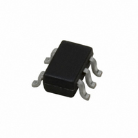
LPV7215MG/NOPB National Semiconductor, LPV7215MG/NOPB Datasheet - Page 12

LPV7215MG/NOPB
Manufacturer Part Number
LPV7215MG/NOPB
Description
IC COMP 1.8V P-P R-R I/O SC70-5
Manufacturer
National Semiconductor
Series
PowerWise®r
Type
General Purposer
Datasheet
1.LPV7215MFNOPB.pdf
(18 pages)
Specifications of LPV7215MG/NOPB
Number Of Elements
1
Output Type
MOS, Push-Pull, Rail-to-Rail
Voltage - Supply
1.8 V ~ 5.5 V
Mounting Type
Surface Mount
Package / Case
6-TSSOP (5 lead), SC-88A, SOT-353
Comparator Type
General Purpose
No. Of Comparators
1
Response Time
4.5µs
Ic Output Type
Push Pull
Supply Current
580nA
Supply Voltage Range
1.8V To 5.5V
Amplifier Case Style
SC-70
Rohs Compliant
Yes
Number Of Elements
1
Technology
CMOS
Input Offset Voltage
3mV
Single Supply Voltage (typ)
3/5V
Dual Supply Voltage (typ)
Not RequiredV
Supply Current (max)
0.00103@5VmA
Power Supply Requirement
Single
Common Mode Rejection Ratio
98dB
Voltage Gain In Db
120dB
Power Supply Rejection Ratio
82dB
Single Supply Voltage (min)
1.8V
Single Supply Voltage (max)
5.5V
Dual Supply Voltage (min)
Not RequiredV
Dual Supply Voltage (max)
Not RequiredV
Operating Temp Range
-40C to 85C
Operating Temperature Classification
Industrial
Mounting
Surface Mount
Pin Count
5
Package Type
SC-70
Lead Free Status / RoHS Status
Lead free / RoHS Compliant
Other names
LPV7215MG
LPV7215MGTR
LPV7215MGTR
Available stocks
Company
Part Number
Manufacturer
Quantity
Price
www.national.com
Application Information
Low supply current and fast propagation delay distinguish the
LPV7215 from other low power comparators.
INPUT STAGE
The LPV7215 has rail-to-rail input common mode voltage
range. It can operate at any differential input voltage within
this limit as long as the differential voltage is greater than zero.
A differential input of zero volts may result in oscillation.
The differential input stage of the comparator is a pair of
PMOS and NMOS transistors, therefore, no current flows into
the device. The input bias current measured is the leakage
current in the MOS transistors and input protection diodes.
This low bias current allows the comparator to interface with
a variety of circuitry and devices with minimal concern about
matching the input resistances.
The input to the comparator is protected from excessive volt-
age by internal ESD diodes connected to both supply rails.
This protects the circuit from both ESD events, as well as sig-
nals that significantly exceed the supply voltages. When this
occurs the ESD protection diodes will become forward biased
and will draw current into these structures, resulting in no in-
put current to the terminals of the comparator. Until this
occurs, there is essentially no input current to the diodes. As
a result, placing a large resistor in series with an input that
may be exposed to large voltages, will limit the input current
but have no other noticeable effect.
OUTPUT STAGE
The LPV7215 has a MOS push-pull rail-to-rail output stage.
The push-pull transistor configuration of the output keeps the
total system power consumption to a minimum. The only cur-
rent consumed by the LPV7215 is the less than 1 µA supply
current and the current going directly into the load. No power
is wasted through the pull-up resistor when the output is low.
The output stage is specifically designed with deadtime be-
tween the time when one transistor is turned off and the other
is turned on (break-before-make) in order to minimize shoot
through currents. The internal logic controls the break-before-
make timing of the output transistors. The break-before-make
delay varies with temperature and power condition.
OUTPUT CURRENT
Even though the LPV7215 uses less than 1 µA supply current,
the outputs are able to drive very large currents. The LPV7215
can source up to 17 mA and can sink up to 19 mA, when
operated at 5V supply. This large current handling capability
allows driving heavy loads directly.
12
RESPONSE TIME
Depending upon the amount of overdrive, the propagation
delay will be typically 6 to 30 µs. The curves showing propa-
gation delay vs. overdrive in the “Typical Characteristics”
section shows the delay time when the input is preset with
100 mV across the inputs and then is driven the other way by
10 mV to 500 mV.
The output signal can show a step during switching depend-
ing on the load. A fast RC time constant due to both small
capacitive and resistive loads will show a significant step in
the output signal. A slow RC time constant due to either a
large resistive or capacitive load will have a clipped corner on
the output signal. The step is observed more prominently dur-
ing a falling transition from high to low.
The plot in Figure 1 shows the output for single 5V supply with
a 100 kΩ resistor. The step is at 1.3V.
The plot in Figure 2 shows the output signal when a 20 pF
capacitor is added as a load. The step is at about 2.5V.
FIGURE 1. Output Signal without Capacitive Load
FIGURE 2. Output Signal with 20 pF Load
20123627
20123628


