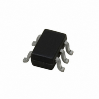
LPV7215MG/NOPB National Semiconductor, LPV7215MG/NOPB Datasheet - Page 14

LPV7215MG/NOPB
Manufacturer Part Number
LPV7215MG/NOPB
Description
IC COMP 1.8V P-P R-R I/O SC70-5
Manufacturer
National Semiconductor
Series
PowerWise®r
Type
General Purposer
Datasheet
1.LPV7215MFNOPB.pdf
(18 pages)
Specifications of LPV7215MG/NOPB
Number Of Elements
1
Output Type
MOS, Push-Pull, Rail-to-Rail
Voltage - Supply
1.8 V ~ 5.5 V
Mounting Type
Surface Mount
Package / Case
6-TSSOP (5 lead), SC-88A, SOT-353
Comparator Type
General Purpose
No. Of Comparators
1
Response Time
4.5µs
Ic Output Type
Push Pull
Supply Current
580nA
Supply Voltage Range
1.8V To 5.5V
Amplifier Case Style
SC-70
Rohs Compliant
Yes
Number Of Elements
1
Technology
CMOS
Input Offset Voltage
3mV
Single Supply Voltage (typ)
3/5V
Dual Supply Voltage (typ)
Not RequiredV
Supply Current (max)
0.00103@5VmA
Power Supply Requirement
Single
Common Mode Rejection Ratio
98dB
Voltage Gain In Db
120dB
Power Supply Rejection Ratio
82dB
Single Supply Voltage (min)
1.8V
Single Supply Voltage (max)
5.5V
Dual Supply Voltage (min)
Not RequiredV
Dual Supply Voltage (max)
Not RequiredV
Operating Temp Range
-40C to 85C
Operating Temperature Classification
Industrial
Mounting
Surface Mount
Pin Count
5
Package Type
SC-70
Lead Free Status / RoHS Status
Lead free / RoHS Compliant
Other names
LPV7215MG
LPV7215MGTR
LPV7215MGTR
Available stocks
Company
Part Number
Manufacturer
Quantity
Price
www.national.com
NON-INVERTING COMPARATOR WITH HYSTERESIS
A non-inverting comparator with hysteresis requires a two re-
sistor network, and a voltage reference (V
input. When V
to switch from low to high, V
V
As soon as V
than V
To make the comparator switch back to it’s low state, V
equal V
culated by
The hysteresis of this circuit is the difference between V
and V
IN1
FIGURE 4. Non-Inverting Comparator with Hysteresis
is calculated by.
IN2
REF
REF
.
, which is given by
before V
O
IN
switches to V
is low, the output is also low. For the output
A
ΔV
will again equal V
IN
= V
CC
IN
, V
CC
must rise up to V
R
A
will step to a value greater
1
/R
2
REF
REF
. V
) at the inverting
IN2
20123642
can be cal-
IN1
IN
20123635
where
must
IN1
14
ZERO CROSSING DETECTOR
In a zero crossing detector circuit, the inverting input is con-
nected to ground and the non-inverting input is connected to
a 100 mV
crosses 0V, the comparator’s output changes state.
To improve switching times and to center the input threshold
to ground a small amount of positive feedback is added to the
circuit. The voltage divider, R
voltage, V
tance, R
V
sistor, R
R
very small (ΔV
output voltage transitions. Diode D
inverting input terminal of the comparator never goes below
approximately −100 mV. As the input terminal goes negative,
D
approximately −700 mV. This sets up a voltage divider with
R
imum negative input overdrive is limited by the current han-
dling ability of D
2
5
1
2
, will be satisfied when V
). The resultant hysteresis established by this network is
will forward bias, clamping the node between R
and R
FIGURE 6. Zero Crossing Detector with Positive
6
1
3
PP
, is made very large with respect to R
1
plus R
preventing V
, at the positive input. By making the series resis-
FIGURE 5. Zero Crossing Detector
AC signal. As the signal at the non-inverting input
1
1
2
< 10 mV) but it is sufficient to insure rapid
.
equal to R
2
from going below ground. The max-
Feedback
IN
4
5
and R
= 0. The positive feedback re-
, the switching condition, V
1
5
is used to insure that the
, establishes a reference
20123649
5
(R
1
and R
6
20123629
= 2000
2
1
to
=


