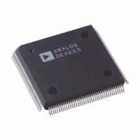
ADV7160KS170 Analog Devices Inc, ADV7160KS170 Datasheet - Page 15

ADV7160KS170
Manufacturer Part Number
ADV7160KS170
Description
IC DAC VIDEO COLOR 96BIT 160MQFP
Manufacturer
Analog Devices Inc
Type
Video DACr
Datasheet
1.ADV7160KS140.pdf
(44 pages)
Specifications of ADV7160KS170
Rohs Status
RoHS non-compliant
Applications
HDTV
Mounting Type
Surface Mount
Package / Case
160-MQFP, 160-PQFP
REV. 0
(Continued from page 1)
The ADV7160/ADV7162 integrates a number of graphic func-
tions onto one device allowing 24-bit direct True-Color (30-bit
Corrected-Color) operation at the maximum screen resolution
of 1600
ADV7162 integrates a 256 30 Color Palette RAM with three
high speed, 10-bit, digital-to analog converters (RGB DACs).
It also contains a user-definable, X-Windows compatible, 64
64
Overlay Palette RAM is also included. The device’s 96-bit Pro-
grammable Pixel Port enables various data formats to be input
to the part. An on-board clock and synchronization circuit
controls all clocking functions for both the part and graphics
subsystem.
There are two video data paths through the ADV7160/ADV7162.
One routes the data from the pixel port through the RAM to the
DACs, the other bypasses the RAM and routes data direct from
the pixel port to the DACs. Either path can be selected on a
pixel by pixel basis. This allows for the overlay of an active
video window on a graphics background.
The on-board palette priority select inputs enable multiple pal-
ette devices to be connected together for use in multipalette and
window applications. The part is controlled and programmed
through the microprocessor (MPU) port.
CIRCUIT DETAILS AND
OPERATION
OVERVIEW
Digital video or pixel data is latched into the ADV7160/ADV7162
over the devices Pixel Port. This data acts as a pointer to on-
board Color Palette RAM. The data at the RAM address pointed
to is latched to the digital-to-analog converters (DACs) and out-
put as an RGB analog video signal.
For the purposes of clarity of description, the ADV7160/ADV7162
is broken down into three separate functional blocks. These are:
1. Pixel Port and Clock Control Circuit
2. MPU Port, Registers and Color Palette
3. Digital-to-Analog Converters and Video Outputs
Pixel Port & Clock Control Circuit
The Pixel Port of the ADV7160/ADV7162 is directly interfaced
to the video/graphics pipeline of a computer graphics subsystem.
It is connected directly or through a gate array to the video
RAM of the systems Frame-Buffer (video memory). The pixel
port on the device consists of:
Color Data
Pixel Controls
Palette Selects
The associated clocking signals for the pixel port include:
Clock Inputs
Clock Outputs
These on-board clock control signals are included to simplify in-
terfacing between the part and the frame buffer. Either two
control input signals CLOCK and CLOCK (ECL Levels) or
2 cursor generator and associated RAM. An on-board
1280 at a refresh rate of 85 Hz. The ADV7160/
RED, GREEN, BLUE
SYNC, BLANK, TRISYNC
PS0
CLOCK, CLOCK, PLL
LOADIN, SCKIN
LOADOUT, PRGCKOUT,
SCKOUT
A-D
, PS1
A-D
REF
,
–15–
one TTL input signal PLL
operational. No additional signals or external glue logic are re-
quired to get the Pixel Port and Clock Control Circuit of the
part operational.
Pixel Port (Color Data)
The ADV7160/ADV7162 has 96 color data inputs. The part
has four (for 4:1 multiplexing) 24-bit wide direct color data in-
puts. These are user programmed to support a number of color
data formats including 24-bit True-Color, 16-bit True-Color,
15-bit True-Color in 4:1 and 2:1 multiplex modes, and 8-bit
Pseudo-Color (see “Multiplexing” section) in 8:1, 4:1 and 2:1
multiplex modes.
Color data is latched into the parts pixel port on every rising
edge of LOADIN (see Timing Waveform, Figure 4). The
required frequency of LOADIN is determined by the multiplex
rate, where
The 30 bits of resolution, associated with the color look-up table
and triple 10-bit DAC, realizes 24-bit True-Color resolution,
while also allowing for the on-board implementation of linear-
ization algorithms, such as Gamma-Correction and Monitor
Callibration. This allows effective 30-bit True-Color operation.
The on-chip video clock controller circuit generates all the inter-
nal clocking and some additional external clocking signals. The
high accuracy, low jitter on board PLL eliminates the need for
an external high speed clock generator. The PLL can be pro-
grammed to produce a pixel clock that is a multiple of the PLL
reference clock.
The ADV7162 is packaged in a standard plastic 160-pin quad
flatpack (QFP).
The ADV7160 is packaged in a plastic 160-pin power quad
flatpack (PQUAD). Superior thermal distribution is achieved by
the inclusion of a copper heatslug, within the standard package
outline, to which the die is attached. This part is ideally suited
for high performance applications where external environmental
conditions are unpredictable and uncontrollable.
f
f
f
LOADIN
LOADIN
LOADIN
Figure 15. Multiplexed Color Inputs for the
ADV7160/ADV7162
GREEN
BLUE
= f
= f
= f
RED
CLOCK
CLOCK
CLOCK
8
8
8
/8
/4
/2
REF
8:1 multiplex mode
4:1 multiplex mode
2:1 multiplex mode
A
B
C
D
ADV7160/ADV7162
are required to get the part
24
24
24
24
MULTIPLEXER
24


