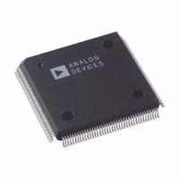
ADV7160KS170 Analog Devices Inc, ADV7160KS170 Datasheet - Page 4

ADV7160KS170
Manufacturer Part Number
ADV7160KS170
Description
IC DAC VIDEO COLOR 96BIT 160MQFP
Manufacturer
Analog Devices Inc
Type
Video DACr
Datasheet
1.ADV7160KS140.pdf
(44 pages)
Specifications of ADV7160KS170
Rohs Status
RoHS non-compliant
Applications
HDTV
Mounting Type
Surface Mount
Package / Case
160-MQFP, 160-PQFP
ADV7160/ADV7162
MPU P
Parameter
t
t
t
t
t
t
t
t
t
t
NOTES
General Notes
1
2
3
Notes on PIXEL PORT
4
5
6
Notes on ANALOG OUTPUTS
7
Notes on MPU PORT
8
9
Specifications subject to change without notice.
TTL input values are 0 to 3 volts, with input rise/fall times
Temperature range (T
Pixel Port consists of the following inputs:
These fixed values for Pipeline Delay are valid under conditions where t
Output delay measured from the 50% point of the rising edge of CLOCK to the 50% point of full-scale transition.
t
t
19
20
21
22
23
24
25
26
27
28
ECL inputs (CLOCK, CLOCK) are V
Timing reference points at 50% for inputs and outputs.
Analog output load
Data-Bus (D0–D9) loaded as shown in Figure 1.
Digital output load for LOADOUT, PRGCKOUT & SCKOUT
Delay is increased.
Output rise/fall time measured between the 10% and 90% points of full-scale transition.
Transition time measured from the 50% point of full scale transition to the output remaining within 2% of the final output value. (Transition time does not include
clock and data feedthrough).
then extrapolated back to remove the effects of charging the 100 pF capacitor. This means that the times t
true values for the device and as such are independent of external loading capacitances.
23
25
5% for all versions
is the LOADOUT Cycle Time and is a function of the Pixel CLOCK Rate and the Multiplexing Mode:
8
9
9
9
and t
and t
Pixel Inputs:
Palette Selects:
Pixel Controls:
Clock Inputs:
Clock Outputs:
2:1 multiplexing;
4:1 multiplexing;
8:1 multiplexing;
24
ORT
26
are measured with the load circuit of Figure 1 and defined as the time required for an output to cross 0.4 V or 2.4 V.
are derived from the measured time taken by the data outputs to change by 0.5 V when loaded with the circuit of Figure 1. The measured numbers are
8,9
10 pF.
MIN
220 MHz
Version
0
10
45
25
5
45
20
5
20
5
RED [A, B, C, D]
PS0 [A, B, C, D];
SYNC, BLANK, TRISYNC, ODD/EVEN
CLOCK, CLOCK, LOADIN, SCKIN
LOADOUT, PRGCKOUT, SCKOUT
to T
= CLOCK
= CLOCK
= CLOCK
MAX
); 0 C to +70 C.
Figure 1. Load Circuit for Databus Access and Relinquish Times
AA
–0.8 V to V
2
4
8
170 MHz
Version
0
10
45
25
5
45
20
5
20
5
GREEN [A, B, C, D]
PS1[A, B, C, D]
= 2
= 4
= 8
AA
–1.8 V, with input rise/fall times
t
t
t
1
1
1
TO OUTPUT
3 ns, measured between the 10% and 90% points.
PIN
ns
ns
ns
30 pF.
140 MHz
Version
0
10
45
25
5
45
20
5
20
5
10
100pF
and -t
BLUE [A, B, C, D]
–4–
11
are met. If either t
2 ns, measured between the 10% and 90% points.
I
I
SOURCE
SINK
Units
ns min
ns min
ns min
ns min
ns min
ns max
ns max
ns min
ns min
ns min
+2.1V
10
or -t
25
and t
11
are not met, the part will operate but the Pipeline
26
Conditions/Comments
R/W, C0, C1 to CE Setup Time
R/W, C0, C1 to CE Hold Time
CE Low Time
CE High Time
CE Asserted to Data-Bus Driven
CE Asserted to Data Valid
CE Disabled to Data-Bus Three-Stated
CE Disabled to Data Invalid
Write Data (D0–D9) Setup Time
Write Data (D0–D9) Hold Time
, quoted in the Timing Characteristics are the
REV. 0


