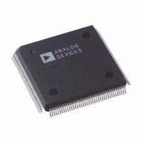
ADV7160KS170 Analog Devices Inc, ADV7160KS170 Datasheet - Page 26

ADV7160KS170
Manufacturer Part Number
ADV7160KS170
Description
IC DAC VIDEO COLOR 96BIT 160MQFP
Manufacturer
Analog Devices Inc
Type
Video DACr
Datasheet
1.ADV7160KS140.pdf
(44 pages)
Specifications of ADV7160KS170
Rohs Status
RoHS non-compliant
Applications
HDTV
Mounting Type
Surface Mount
Package / Case
160-MQFP, 160-PQFP
ADV7160/ADV7162
REGISTER PROGRAMMING
The following section describes each register, including Address
Register, Mode Register and each of the Control Registers in
terms of its configuration.
Address Register (A10–A0)
As illustrated in the previous tables, the C1 and C0 control in-
puts, in conjunction with this address register specify which
control register, or color palette location is accessed by the
MPU port. The Address Register is 11 bits wide and can be
read from as well as written to. To access the Address Register,
two consecutive MPU accesses with C1 and C0 set to Logic “0”
are required. The first one accesses the low byte; and when a
second access of the same type is performed, i.e., two consecu-
tive reads or two consecutive writes, the high byte is accessed.
If the type of access is changed, or if an access to a different reg-
ister is inserted between the first and the second, then the sec-
ond access will access the low byte again. When writing to or
reading from the color palette on a sequential basis, only the
start address needs to be written. After a red, green and blue
write sequence, the address register is automatically incremented.
Mode Register (MR1)
The mode register is a 10-bit wide register. However for pro-
gramming purposes, it may be considered as an 8-bit wide regis-
ter (MR19 and MR18 are both reserved). It is denoted as
MR17–MR10 for simplification purposes.
Figure 39 shows the various operations under the control of the
mode register. This register can be read from as well written to.
In read mode, if MR19 and MR18 are read back, they are both
returned as zeros.
MODE REGISTER BIT DESCRIPTION
Reset Control (MR10)
This bit is used to reset the pixel port sampling sequence. This
ensures that the pixel sequence ABCD starts at A. It is reset by
writing a “1” followed by a “0” followed by a “1.” This bit must
run this cycle during the initialization sequence.
*
THESE BITS ARE READ-ONLY
RESERVED BITS.
A READ CYCLE WILL RETURN
ZEROS "00."
MR19
RESERVED*
MR18
MATCH BITS CONTROL
MR16
MR17
PALETTE SELECT
Figure 39. Mode Register 1 (MR1) (MR19–MR10)
MR17
PS0
PS1
MR14 MR13
0
0
1
1
MR16
OPERATIONAL MODE CONTROL
0
1
0
1
MR15
CALIBRATE
NORMAL OPERATION
RESERVED
RESERVED
RESERVED
MR15
LOADIN
–26–
RAM-DAC Resolution Control (MR11)
When this is programmed with a “1,” the RAM is 30 bits deep
(10 bits each for red, green and blue), and each of the three
DACs is configured for 10-bit resolution. When MR11 is pro-
grammed with a “0,” the RAM is 24 bits deep (8 bits each for
red, green and blue), and the DACs are configured for 8-bit
resolution. The two LSBs of the 10-bit DACs are pulled down
to zero in 8-bit RAM-DAC mode.
MPU Data Bus Width (MR12)
This bit determines the width of the MPU port. It is configured
as either a 10-bit wide (D9–D0) or 8-bit wide (D7–D0) bus.
Ten-bit data can be written to the device when configured 8-bit
wide mode. The 8 MSBs are first written on D7–D0, then the
two LSBs are written over D1–D0. Bits D9–D8 are zeros in 8-
bit mode.
Operational Mode Control (MR14–MR13)
When MR14 and MR13 are “0” the part operates in normal
mode.
Calibrate LOADIN (MR15)
This bit automatically calibrates the on-board LOADIN/
LOADOUT synchronization circuit. A “0” to “1” transition
initiates calibration. This bit is set to “0” in normal operation.
See “Pipeline Delay & Calibration” section. This bit must run
this cycle during the initialization sequence.
Palette Select Match Bits Control (MR17–MR16)
These bits allow multiple palette devices to work together.
When bits PS1 and PS0 match MR17 and MR16 respectively,
the device is selected. If these bits do not match, the device is
not selected and the analog video outputs drive 0 mA. See
“Palette Priority Select Inputs” section.
CONTROL REGISTERS
A large bank of registers plus the 64 64 cursor image can be
accessed through the Control Register. Access is made first by
writing the Address Register with the appropriate address to
point to the particular Control Register (see Figure 34), and
PCR4
MR14
MR12
MR13
0
1
MPU DATA BUS
8-BIT (D7–D0)
10-BIT (D9–D0)
WIDTH
RESOLUTION CONTROL
MR11
MR12
0
1
RAM-DAC
8-BIT
10-BIT
MR11
MR10
CONTROL
RESET
MR10
REV. 0


