74LVT16244MTD Fairchild Semiconductor, 74LVT16244MTD Datasheet - Page 4
74LVT16244MTD
Manufacturer Part Number
74LVT16244MTD
Description
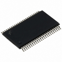
IC BUFF DVR TRI-ST 16BIT 48TSSOP
Manufacturer
Fairchild Semiconductor
Series
74LVTr
Datasheet
1.74LVT16244MTDX.pdf
(7 pages)
Specifications of 74LVT16244MTD
Logic Type
Buffer/Line Driver, Non-Inverting
Number Of Elements
4
Number Of Bits Per Element
4
Current - Output High, Low
32mA, 64mA
Voltage - Supply
2.7 V ~ 3.6 V
Operating Temperature
-40°C ~ 85°C
Mounting Type
Surface Mount
Package / Case
48-TSSOP
Logic Device Type
Buffer, Non Inverting
Supply Voltage Range
2.7V To 3.6V
Logic Case Style
TSSOP
No. Of Pins
48
Operating Temperature Range
-65°C To +150°C
Svhc
No SVHC (15-Dec-2010)
Rohs Compliant
Yes
Lead Free Status / RoHS Status
Lead free / RoHS Compliant
Available stocks
Company
Part Number
Manufacturer
Quantity
Price
Company:

Part Number:
74LVT16244MTD
Manufacturer:
FAIRCHILD
Quantity:
319
Part Number:
74LVT16244MTD
Manufacturer:
FAIRCHILD/仙童
Quantity:
20 000
Company:
Part Number:
74LVT16244MTDX
Manufacturer:
SIPEX
Quantity:
10 000
Part Number:
74LVT16244MTDX
Manufacturer:
FAIRCHILD/仙童
Quantity:
20 000


www.fairchildsemi.com
V
V
t
t
t
t
t
t
t
t
I
I
I
I
'
C
C
PLH
PHL
PZH
PZL
PHZ
PLZ
OSHL
OSLH
DC Electrical Characteristics
CCH
CCL
CCZ
CCZ
Note 5: Applies to bushold versions only (LVTH16244).
Note 6: An external driver must source at least the specified current to switch from LOW-to-HIGH.
Note 7: An external driver must sink at least the specified current to switch from HIGH-to-LOW.
Note 8: This is the increase in supply current for each input that is at the specified voltage level rather than V
Dynamic Switching Characteristics
Note 9: Characterized in SSOP package. Guaranteed parameter, but not tested.
Note 10: Max number of outputs defined as (n). n
AC Electrical Characteristics
Note 11: Skew is defined as the absolute value of the difference between the actual propagation delay for any two separate outputs of the same device. The
specification applies to any outputs switching in the same direction, either HIGH-to-LOW (t
Capacitance
Note 12: Capacitance is measured at frequency f
OLP
OLV
I
Symbol
Symbol
IN
OUT
Symbol
Symbol
CC
Quiet Output Maximum Dynamic V
Quiet Output Minimum Dynamic V
Propagation Delay Data to Output
Output Enable Time
Output Disable Time
Output to Output Skew
(Note 11)
Input Capacitance
Output Capacitance
Power Supply Current
Power Supply Current
Power Supply Current
Power Supply Current
Increase in Power Supply Current
(Note 8)
Parameter
(Note 12)
Parameter
Parameter
Parameter
OL
1 data inputs are driven 0V to 3V. Output under test held LOW.
OL
1 MHz, per MIL-STD-883, Method 3012.
V
(V)
3.3
3.3
CC
(Continued)
V
V
CC
CC
V
(V)
3.6
3.6
3.6
3.6
3.6
0V, V
3.0V, V
CC
Min
(Note 9)
4
I
Min
1.2
1.2
1.2
1.2
2.0
1.5
V
O
CC
0V or V
T
T
Conditions
A
0V or V
Min
A
3.3V
Typ
0.8
0.8
OSHL
CC
25
40
r
q
q
CC
C
C to
) or LOW-to-HIGH (t
C
0.3V
T
Max
L
3.5
3.5
4.0
5.0
4.7
4.2
1.0
A
Max
0.19
0.19
0.19
5.0
0.2
50 pF, R
85
Max
40
q
C
q
C to
CC
L
or GND.
85
Units
500
Min
1.2
1.2
1.2
1.2
2.0
1.5
OSLH
mA
mA
mA
mA
mA
Units
q
C
:
V
V
V
).
CC
Typical
Outputs High
Outputs Low
Outputs Disabled
V
Outputs Disabled
One Input at V
Other Inputs at V
2.7V
CC
4
8
d
C
Max
3.9
3.9
5.0
6.5
5.2
4.4
1.0
V
L
O
Conditions
d
50 pF, R
Conditions
(Note 10)
(Note 10)
5.5V,
CC
CC
L
Units
0.6V
or GND
pF
pF
Units
500
ns
ns
ns
ns
:
Related parts for 74LVT16244MTD
Image
Part Number
Description
Manufacturer
Datasheet
Request
R

Part Number:
Description:
IC BUFF/DVR TRI-ST DUAL 20TSSOP
Manufacturer:
Fairchild Semiconductor
Datasheet:
Part Number:
Description:
IC TRANSCVR TRI-ST 8BIT 20TSSOP
Manufacturer:
Fairchild Semiconductor
Datasheet:
Part Number:
Description:
IC LATCH TRANSP OCT 3ST 20TSSOP
Manufacturer:
Fairchild Semiconductor
Datasheet:

Part Number:
Description:
IC LATCH TRANSP 16BIT 48TSSOP
Manufacturer:
Fairchild Semiconductor
Datasheet:

Part Number:
Description:
IC BUFF/DVR TRI-ST DUAL 20SOIC
Manufacturer:
Fairchild Semiconductor
Datasheet:
Part Number:
Description:
IC BUFF DVR TRI-ST 16BIT 48TSSOP
Manufacturer:
Fairchild Semiconductor
Datasheet:

Part Number:
Description:
IC TRANSCVR TRI-ST 16BIT 48TSSOP
Manufacturer:
Fairchild Semiconductor
Datasheet:

Part Number:
Description:
IC BUFF TRI-ST QD N-INV 14SSOP
Manufacturer:
NXP Semiconductors
Datasheet:

Part Number:
Description:
IC TRANSCVR TRI-ST 8BIT 20SSOP
Manufacturer:
NXP Semiconductors
Datasheet:

Part Number:
Description:
IC BUFF/DVR TRI-ST DUAL 20TSSOP
Manufacturer:
NXP Semiconductors
Datasheet:

Part Number:
Description:
IC BUFF TRI-ST QD N-INV 14SOICN
Manufacturer:
NXP Semiconductors
Datasheet:
Part Number:
Description:
IC TRANSCEIVER 8BIT INV 20TSSOP
Manufacturer:
NXP Semiconductors
Datasheet:
Part Number:
Description:
IC TRANSCVR TRI-ST 16BIT 48TSSOP
Manufacturer:
Fairchild Semiconductor
Datasheet:
Part Number:
Description:
IC BUFF/DVR TRI-ST DUAL 20TSSOP
Manufacturer:
Fairchild Semiconductor
Datasheet:
Part Number:
Description:
IC BUFF/DVR TRI-ST DUAL 20TSSOP
Manufacturer:
Fairchild Semiconductor
Datasheet: