74VCX32244GX Fairchild Semiconductor, 74VCX32244GX Datasheet
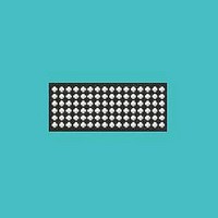
IC BUFF DVR 32BIT LOW V 96FBGA

74VCX32244GX

Manufacturer Part Number
74VCX32244GX
Description
IC BUFF DVR 32BIT LOW V 96FBGA
Manufacturer
Fairchild Semiconductor
Series
74VCXr
Datasheet

Specifications of 74VCX32244GX

Logic Type
Buffer/Line Driver, Non-Inverting
Number Of Elements
8
Number Of Bits Per Element
4
Current - Output High, Low
24mA, 24mA
Voltage - Supply
1.2 V ~ 3.6 V
Operating Temperature
-40°C ~ 85°C
Mounting Type
Surface Mount
Package / Case
96-LFBGA
Logic Family
VCX
Number Of Channels Per Chip
32
Polarity
Non-Inverting
Supply Voltage (max)
3.6 V
Supply Voltage (min)
1.2 V
Maximum Operating Temperature
+ 85 C
Mounting Style
SMD/SMT
High Level Output Current
- 24 mA
Low Level Output Current
24 mA
Minimum Operating Temperature
- 40 C
Number Of Lines (input / Output)
32 / 3
Output Type
3-State
Propagation Delay Time
6 ns at 1.8 V, 3 ns at 2.5 V, 2.5 ns at 3.3 V
Lead Free Status / RoHS Status
Lead free / RoHS Compliant

Available stocks

Company
Part Number
Manufacturer
Quantity
Price
Part Number:
74VCX32244GX
Manufacturer:
Fairchild Semiconductor
Quantity:
1 832
Part Number:
74VCX32244GX
Quantity:
53
Part Number:
74VCX32244GX
Manufacturer:
Fairchild Semiconductor
Quantity:
10 000
© 2002 Fairchild Semiconductor Corporation
74VCX32244G
(Note 2)(Note 3)
74VCX32244
Low Voltage 32-Bit Buffer/Line Driver
with 3.6V Tolerant Inputs and Outputs
General Description
The VCX32244 contains thirty-two non-inverting buffers
with 3-STATE outputs to be employed as a memory and
address driver, clock driver, or bus oriented transmitter/
receiver. The device is nibble (4-bit) controlled. Each nibble
has separate 3-STATE control inputs which can be shorted
together for 8-bit, 16-bit or full 32-bit operation.
The 74VCX32244 is designed for low voltage (1.2V to
3.6V) V
The 74VCX32244 is fabricated with an advanced CMOS
technology to achieve high speed operation while maintain-
ing low CMOS power dissipation.
Ordering Code:
Note 2: Ordering code “G” indicates Trays.
Note 3: Devices also available in Tape and Reel. Specify by appending the suffix letter “X” to the ordering code.
Logic Symbol
Order Number
CC
applications with I/O capability up to 3.6V.
Package Number
BGA96A
96-Ball Fine-Pitch Ball Grid Array (FBGA), JEDEC MO-205, 5.5mm Wide
DS500416
Features
Note 1: To ensure the high-impedance state during power up or power
down, OE should be tied to V
value of the resistor is determined by the current-sourcing capability of the
driver.
1.2V to 3.6V V
3.6V tolerant inputs and outputs
t
Power-off high impedance inputs and outputs
Supports live insertion and withdrawal (Note 1)
Static Drive (I
Uses patented noise/EMI reduction circuitry
Latch-up performance exceeds 300 mA
ESD performance:
Packages in plastic Fine-Pitch Ball Grid Array (FBGA)
PD
2.5 ns max for 3.0V to 3.6V V
Human body model
Machine model
24 mA @ 3.0V V
Package Description
OH
CC
/I
OL
supply operation
)
200V
CC
CC
2000V
through a pull-up resistor; the minimum
September 2000
Revised November 2002
CC
www.fairchildsemi.com

Related parts for 74VCX32244GX

74VCX32244GX Summary of contents

Page 1

... Fine-Pitch Ball Grid Array (FBGA), JEDEC MO-205, 5.5mm Wide (Note 2)(Note 3) Note 2: Ordering code “G” indicates Trays. Note 3: Devices also available in Tape and Reel. Specify by appending the suffix letter “X” to the ordering code. Logic Symbol © 2002 Fairchild Semiconductor Corporation Features 1.2V to 3.6V V supply operation CC 3 ...

Page 2

Connection Diagram (Top Thru View) Pin Descriptions Pin Names Description OE Output Enable Input (Active LOW –I Inputs –O Outputs 0 31 FBGA Pin Assignments ...

Page 3

Functional Description The 74VCX32244 contains thirty-two non-inverting buffers with 3-STATE outputs. The device is nibble (4 bits) con- trolled with each nibble functioning identically, but indepen- dent of each other. The control pins may be shorted together to obtain full ...

Page 4

Absolute Maximum Ratings Supply Voltage ( Input Voltage ( Output Voltage ( Outputs 3-STATED Outputs Active (Note 5) 0. Input Diode Current ( Output ...

Page 5

DC Electrical Characteristics Symbol Parameter V LOW Level Output Voltage OL I Input Leakage Current I I 3-STATE Output Leakage OZ I Power-OFF Leakage Current OFF I Quiescent Supply Current CC I Increase in I per Input CC CC Note ...

Page 6

Dynamic Switching Characteristics Symbol Parameter V Quiet Output Dynamic Peak V OLP OL V Quiet Output Dynamic Valley V OLV OL V Quiet Output Dynamic Valley V OHV OH Capacitance Symbol Parameter C Input Capacitance IN C Output Capacitance OUT ...

Page 7

AC Loading and Waveforms (V TEST PLH PHL PZL PLZ PZH PHZ FIGURE 2. Waveform for Inverting and Non-Inverting Functions FIGURE 3. 3-STATE Output High Enable and Disable Times for Low ...

Page 8

AC Loading and Waveforms (V TEST PLH PHL PZL PLZ PZH PHZ FIGURE 6. Waveform for Inverting and Non-Inverting Functions FIGURE 7. 3-STATE Output High Enable and Disable Times for Low ...

Page 9

Physical Dimensions inches (millimeters) unless otherwise noted 96-Ball Fine-Pitch Ball Grid Array (FBGA), JEDEC MO-205, 5.5mm Wide Fairchild does not assume any responsibility for use of any circuitry described, no circuit patent licenses are implied and Fairchild reserves the right ...

Related keywords