74VCX164245MTDX Fairchild Semiconductor, 74VCX164245MTDX Datasheet

IC TRANSCEIVER 16BIT 48TSSOP

74VCX164245MTDX

Manufacturer Part Number
74VCX164245MTDX
Description
IC TRANSCEIVER 16BIT 48TSSOP
Manufacturer
Fairchild Semiconductor
Series
74VCXr
Datasheet

Specifications of 74VCX164245MTDX

Logic Type
Transceiver, Non-Inverting
Number Of Elements
2
Number Of Bits Per Element
8
Operating Temperature
-40°C ~ 85°C
Mounting Type
Surface Mount
Package / Case
48-TSSOP
Number Of Circuits
1
Logic Family
74VC
Polarity
Non-Inverting
Output Type
3-State
Propagation Delay Time
6.2 ns
High Level Output Current
- 24 mA
Low Level Output Current
24 mA
Supply Voltage (max)
2.7 V, 3.6 V
Maximum Operating Temperature
+ 85 C
Mounting Style
SMD/SMT
Minimum Operating Temperature
- 40 C
Supply Voltage (min)
1.65 V, 2.3 V
Lead Free Status / RoHS Status
Lead free / RoHS Compliant
Voltage - Supply
-
Current - Output High, Low
-
Lead Free Status / Rohs Status
Lead free / RoHS Compliant
© 2005 Fairchild Semiconductor Corporation
74VCX164245G
(Note 2)(Note 3)
74VCX164245MTD
(Note 3)
74VCX164245
Low Voltage 16-Bit Dual Supply Translating Transceiver
with 3-STATE Outputs
General Description
The VCX164245 is a dual supply, 16-bit translating trans-
ceiver that is designed for two way asynchronous commu-
nication between busses at different supply voltages by
providing true signal translation. The supply rails consist of
V
3.6V and V
1.65V to 2.7V. (V
for proper device operation.) This dual supply design
allows for translation from 1.8V to 2.5V busses to busses at
a higher potential, up to 3.3V.
The Transmit/Receive (T/R) input determines the direction
of data flow. Transmit (active-HIGH) enables data from A
Ports to B Ports. Receive (active-LOW) enables data from
B Ports to A Ports. The Output Enable (OE) input, when
HIGH, disables both A and B Ports by placing them in a
High-Z condition. The A Port interfaces with the lower volt-
age bus (1.8V
higher voltage bus (2.7V
designed so that the control pins (T/R
by V
The 74VCX164245 is suitable for mixed voltage applica-
tions such as notebook computers using a 1.8V CPU and
3.3V peripheral components. It is fabricated with an
Advanced CMOS technology to achieve high speed opera-
tion while maintaining low CMOS power dissipation.
Ordering Code:
Note 2: Ordering Code “G” indicates Trays.
Note 3: Device also available in Tape and Reel. Specify by appending suffix letter “X” to the ordering code.
Logic Diagram
CCB
Order Number
CCB
, which is the higher potential rail operating at 2.3V to
.
CCA
, which is the lower potential rail operating at

CCA
2.5V). The B Port interfaces with the
Package Number
must be less than or equal to V
BGA54A
MTD48

3.3V). Also the VCX164245 is
n
, OE
54-Ball Fine-Pitch Ball Grid Array (FBGA), JEDEC MO-205, 5.5mm Wide
48-Lead Thin Shrink Small Outline Package (TSSOP), JEDEC MO-153, 6.1mm Wide
n
) are supplied
DS500159
CCB
Features
Note 1: To ensure the high impedance state during power up or power
down, OE
value of the resistor is determined by the current sourcing capability of the
driver.
Bidirectional interface between busses ranging from
1.65V to 3.6V
Supports Live Insertion and Withdrawal (Note 1)
Static Drive (I
Uses patented noise/EMI reduction circuitry
Functionally compatible with 74 series 16245
Latchup performance exceeds 300 mA
ESD performance:
Also packaged in plastic Fine-Pitch Ball Grid Array
(FBGA)
r
r
r
Human Body Model
Machine model
24 mA @ 3.0V V
18 mA @ 2.3V V
6 mA @ 1.65V V
n
Package Description
should be tied to V
OH
/I
OL
!
200V
)
CC
CC
CCB
CC
!
2000V
through a pull up resistor. The minimum
March 2000
Revised June 2005
www.fairchildsemi.com

Related parts for 74VCX164245MTDX

74VCX164245MTDX Summary of contents

Page 1

... Note 2: Ordering Code “G” indicates Trays. Note 3: Device also available in Tape and Reel. Specify by appending suffix letter “X” to the ordering code. Logic Diagram © 2005 Fairchild Semiconductor Corporation Features Bidirectional interface between busses ranging from 1.65V to 3.6V Supports Live Insertion and Withdrawal (Note 1) ...

Page 2

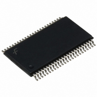
Connection Diagrams Pin Assignment for TSSOP Pin Assignment for FBGA (Top Through View) Translator Power Up Sequence Recommendations To guard against power up problems, some simple guide- lines need to be adhered to. The VCX164245 is designed so that the ...

Page 3

Logic Diagrams Please note that these diagrams are provided only for the understanding of logic operations and should not be used to estimate propagation delays. 3 www.fairchildsemi.com ...

Page 4

Absolute Maximum Ratings Supply Voltage V CCA V CCB DC Input Voltage ( Output Voltage (V ) I/O Outputs 3-STATE Outputs Active (Note 0. 0. Input Diode ...

Page 5

DC Electrical Characteristics (1.65V  V Symbol Parameter V HIGH Level A IHA n V Input Voltage B , T/R, OE IHB n V LOW Level A ILA n V Input Voltage B , T/R, OE ILB n V HIGH ...

Page 6

AC Electrical Characteristics Symbol Parameter Propagation Delay PHL PLH Propagation Delay PHL PLH Output Enable Time PZL PZH Output ...

Page 7

AC Loading and Waveforms TEST PLH PHL PZL PLZ PZH PHZ FIGURE 2. Waveform for Inverting and Non-inverting Functions FIGURE 3. 3-STATE Output High Enable and Disable Times for Low Voltage ...

Page 8

Physical Dimensions inches (millimeters) unless otherwise noted 54-Ball Fine-Pitch Ball Grid Array (FBGA), JEDEC MO-205, 5.5mm Wide Package Number BGA54A 8 www.fairchildsemi.com ...

Page 9

Physical Dimensions inches (millimeters) unless otherwise noted (Continued) 48-Lead Thin Shrink Small Outline Package (TSSOP), JEDEC MO-153, 6.1mm Wide Fairchild does not assume any responsibility for use of any circuitry described, no circuit patent licenses are implied and Fairchild reserves ...

Related keywords