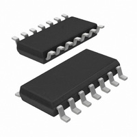
74AHC74D,118 NXP Semiconductors, 74AHC74D,118 Datasheet - Page 4

74AHC74D,118
Manufacturer Part Number
74AHC74D,118
Description
IC DUAL D F-F POS-EDGE 14-SOIC
Manufacturer
NXP Semiconductors
Series
74AHCr
Type
D-Typer
Datasheet
1.74AHC74D118.pdf
(18 pages)
Specifications of 74AHC74D,118
Package / Case
14-SOIC (3.9mm Width), 14-SOL
Function
Set(Preset) and Reset
Output Type
Differential
Number Of Elements
2
Number Of Bits Per Element
1
Frequency - Clock
75MHz
Delay Time - Propagation
7.4ns
Trigger Type
Positive Edge
Current - Output High, Low
8mA, 8mA
Voltage - Supply
2 V ~ 5.5 V
Operating Temperature
-40°C ~ 125°C
Mounting Type
Surface Mount
Number Of Circuits
2
Logic Family
AHC
Logic Type
D-Type Edge Triggered Flip-Flop
Polarity
Inverting/Non-Inverting
Input Type
Single-Ended
Propagation Delay Time
3.7 ns at 5 V
High Level Output Current
- 8 mA
Supply Voltage (max)
5.5 V
Maximum Operating Temperature
+ 125 C
Mounting Style
SMD/SMT
Minimum Operating Temperature
- 40 C
Supply Voltage (min)
2 V
Lead Free Status / RoHS Status
Lead free / RoHS Compliant
Lead Free Status / RoHS Status
Lead free / RoHS Compliant, Lead free / RoHS Compliant
Other names
568-4458-2
74AHC74D-T
74AHC74D-T
935263078118
74AHC74D-T
74AHC74D-T
935263078118
NXP Semiconductors
5. Pinning information
Table 2.
74AHC_AHCT74_5
Product data sheet
Symbol
1RD
1D
1CP
1SD
1Q
1Q
GND
2Q
2Q
2SD
2CP
2D
2RD
V
Fig 5.
CC
Pin configuration SO14 and TSSOP14
Pin description
GND
1RD
1CP
1SD
1Q
1Q
1D
Pin
1
2
3
4
5
6
7
8
9
10
11
12
13
14
5.1 Pinning
5.2 Pin description
1
2
3
4
5
6
7
74
001aac449
Description
asynchronous reset direct input (active LOW)
data input
clock input (LOW to HIGH, edge-triggered)
asynchronous set direct input (active LOW)
true flip-flop output
complement flip-flop output
ground (0 V)
complement flip-flop output
true flip-flop output
asynchronous set direct input (active LOW)
clock input (LOW to HIGH, edge-triggered)
data input
asynchronous reset direct input (active LOW)
supply voltage
14
13
12
11
10
9
8
V
2RD
2D
2CP
2SD
2Q
2Q
CC
Rev. 05 — 9 June 2008
Dual D-type flip-flop with set and reset; positive-edge trigger
Fig 6.
(1)
The die substrate is attached to this pad using
conductive die attach material. It can not be used
as supply pin or input.
Pin configuration DHVQFN14
74AHC74; 74AHCT74
index area
terminal 1
1CP
1SD
1D
1Q
1Q
Transparent top view
2
3
4
5
6
GND
74
(1)
13
12
11
10
9
001aac450
© NXP B.V. 2008. All rights reserved.
2RD
2D
2CP
2SD
2Q
4 of 18


